Technique for improving static random-access memory sense amplifier voltage differential

a random access memory and amplifier technology, applied in static storage, information storage, digital storage, etc., can solve the problems of differential between, accuracy and speed of i/o circuit, introduction of unpredictable voltage drops, etc., to accurately and quickly determine the logical value output, the read accuracy and speed of the memory module is less sensitive.

Active Publication Date: 2015-03-24
NVIDIA CORP
View PDF5 Cites 2 Cited by
  • Summary
  • Abstract
  • Description
  • Claims
  • Application Information

AI Technical Summary

Benefits of technology

[0008]One advantage of the disclosed technique is that the voltage differential between the first bit line and the second bit line is preserved across the logic gates, enabling the sense amplifier to accurately and quickly determine the logical value output on the bit lines based on that preserved voltage differential. Accordingly, the read accuracy and speed of the memory module is less sensitive to process variations and supply voltage reductions that would otherwise degrade that voltage differential.

Problems solved by technology

One weakness of the approach described above is that the sense amplifier requires a large voltage differential between the sense nodes in order to accurately and quickly determine whether that differential represents a “0” or a “1.” However, the voltage differential between the sense nodes, and therefore the read accuracy and speed of the I / O circuit in general, is sensitive to several factors.
This issue is compounded by the fact that manufacturing differences across PMOSs may introduce unpredictable voltage drops across different PMOSs.
In sum, the read accuracy and speed of conventional I / O circuits is limited by the voltage differential detected at the sense nodes of the sense amplifier.

Method used


Image

  • Technique for improving static random-access memory sense amplifier voltage differential
  • Technique for improving static random-access memory sense amplifier voltage differential
  • Technique for improving static random-access memory sense amplifier voltage differential

Examples


Embodiment Construction

[0014]In the following description, numerous specific details are set forth to provide a more thorough understanding of the present invention. However, it will be apparent to one of skill in the art that the present invention may be practiced without one or more of these specific details. In other instances, well-known features have not been described in order to avoid obscuring the present invention.

System Overview

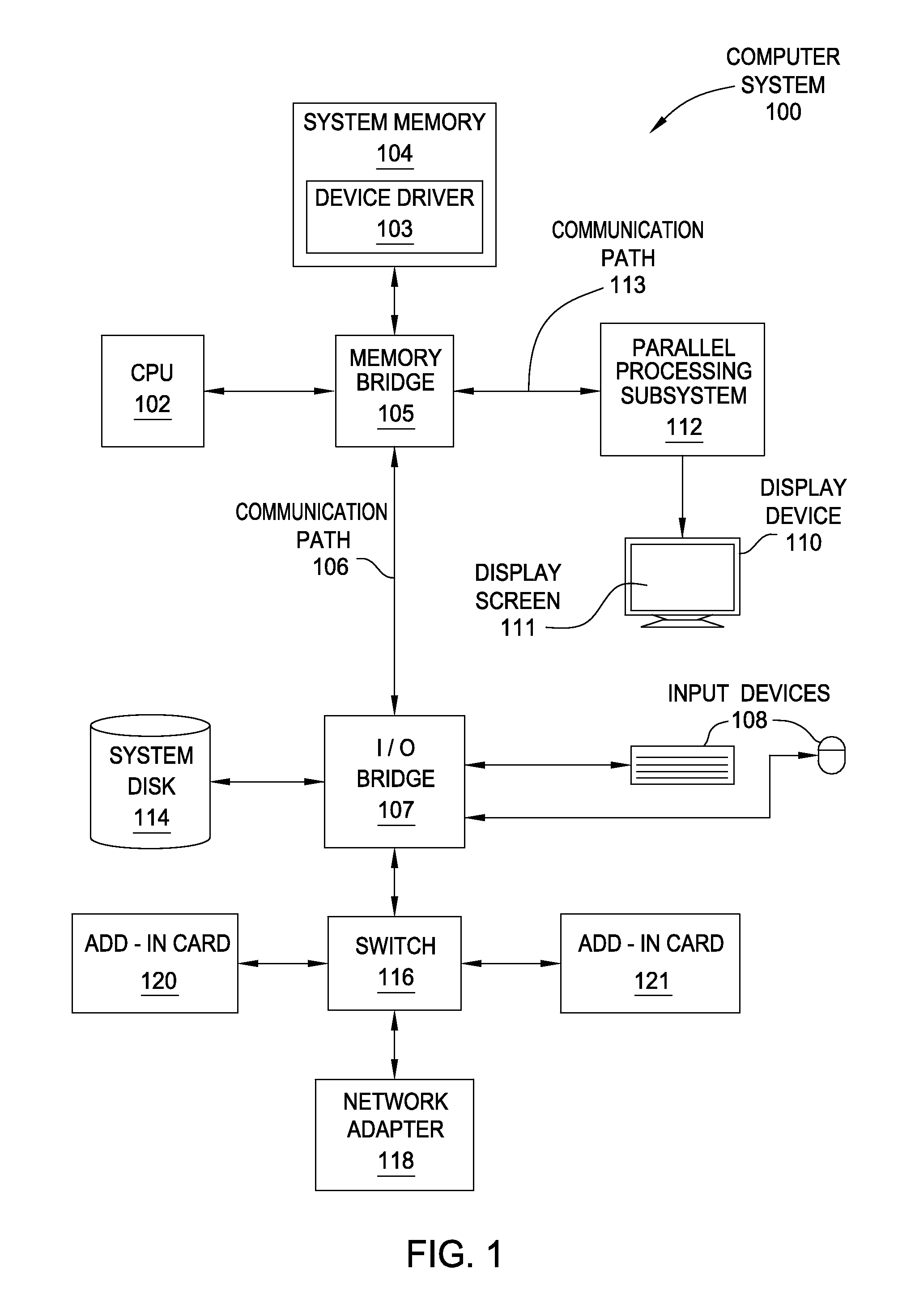
[0015]FIG. 1 is a block diagram that illustrates a computer system 100 configured to implement one or more aspects of the present invention. Computer system 100 includes a central processing unit (CPU) 102 and a system memory 104 that includes a device driver 103. CPU 102 and system memory 104 communicate via an interconnection path that may include a memory bridge 105. Memory bridge 105, which may be, e.g., a Northbridge chip, is connected via a bus or other communication path 106 (e.g., a HyperTransport link) to an input / output (I / O) bridge 107. I / O bridge 107, which ma...


PUM


Abstract

A static random-access memory (SRAM) module includes a column select (RSEL) driver coupled to an input / output (I / O) circuit by an RSEL line. The I / O circuit is configured to read bit line signals from a bit cell within the SRAM module. During a read operation, the RSEL driver pulls the RSEL line to zero in order to cause p-type metal-oxide-semiconductors (PMOSs) within the I / O circuit to sample the bit line signals output by the bit cell. In response, an aggressor driver drives the RSEL line to a negative voltage, thereby reducing the resistance of the PMOSs within the I / O circuit.

Description

BACKGROUND OF THE INVENTION[0001]1. Field of the Invention[0002]The present invention generally relates to static random-access memory (SRAM), and, more specifically, a technique for improving SRAM sense amplifier voltage differential.[0003]2. Description of the Related Art[0004]A conventional SRAM module typically includes a collection of bit cells, where each bit cell is configured to store a logical value (e.g., a “0” or a “1”). During a read operation, a given bit cell outputs two voltage signals on two corresponding bit lines. Each bit line is coupled to a different p-type metal-oxide-semiconductor (PMOS) within an input / output (I / O) circuit residing downstream of the bit cell. The SRAM module causes the I / O circuit to sample the two voltage signals by asserting a column select signal to the two PMOSs. In response to the column select signal, each PMOS conducts a voltage to a sense amplifier also residing within the I / O circuit. The sense amplifier is configured to receive the ...

Claims


Application Information

Patent Timeline
Patent Type & Authority Patents(United States)
IPC IPC(8): G11C7/02G11C7/06G11C7/12G11C11/419
CPCG11C7/062G11C7/065G11C7/12G11C11/419
Inventor HUANG, YONGCHANGMA, JIPINGSHEN, DEMI
Owner NVIDIA CORP
Why Eureka
Try Eureka