Light-emitting diode package

a technology of light-emitting diodes and diodes, which is applied in the direction of semiconductor devices, semiconductor/solid-state device details, electrical apparatus, etc., can solve the problems of complex processes and/or several substrates, and achieve the effect of maximizing light extraction

Active Publication Date: 2015-05-12
SUZHOU LEKIN SEMICON CO LTD
View PDF13 Cites 1 Cited by
  • Summary
  • Abstract
  • Description
  • Claims
  • Application Information

AI Technical Summary

Benefits of technology

[0010]Therefore, embodiments disclosed herein provide an LED package having an LED with a desired slope angle relative to the bottom surface of a cavity on the package to reflect light irradiated through a lateral side of the LED, thus maximizing light extraction.

Problems solved by technology

The preparation of the LED chip and the packaging thereof proceed independently, in turn causing problems of requiring complex processes and / or several substrates.

Method used


Image

  • Light-emitting diode package
  • Light-emitting diode package
  • Light-emitting diode package

Examples


Embodiment Construction

[0023]Prior to description of the embodiments, it will be understood that when an element such as a layer (film), region, pattern, or structure is referred to as being formed “on” or “under” another element, such as a substrate, layer (film), region, pad, or pattern, it can be directly “on” or “under” the other element or be indirectly formed with intervening elements therebetween. Further, “on” or “under” of each layer will be described based on illustration in the drawings.

[0024]In the drawings, thicknesses and / or sizes of respective layers may be enlarged, omitted or schematically illustrated for convenience of explanation or clarity. In addition, sizes of respective elements may not entirely reflect the real size thereof. Further, the same reference numbers will be used throughout the drawings to refer to the same or like parts.

[0025]Hereinafter, the present invention will be described in more detail with reference to the annexed drawings.

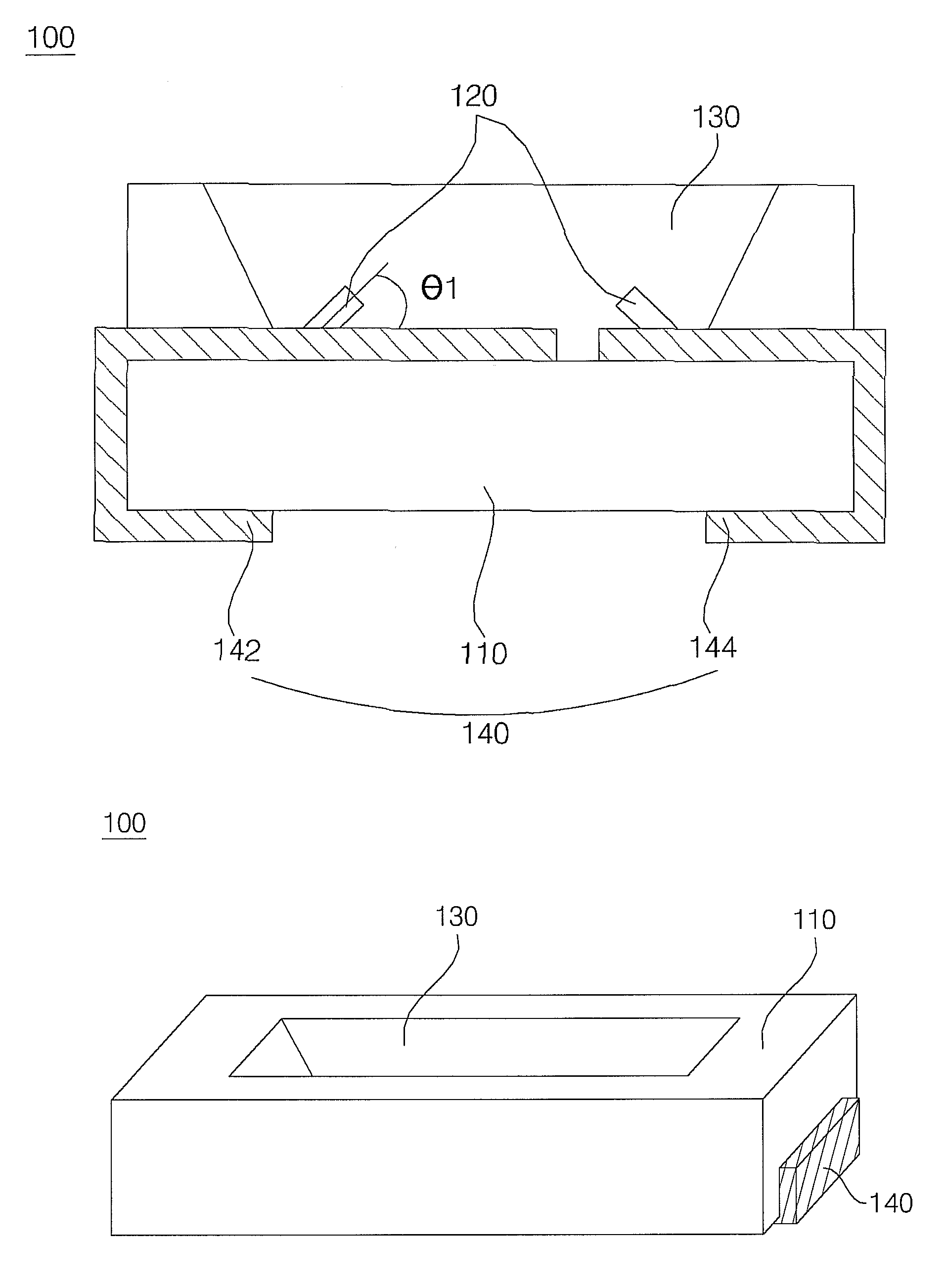
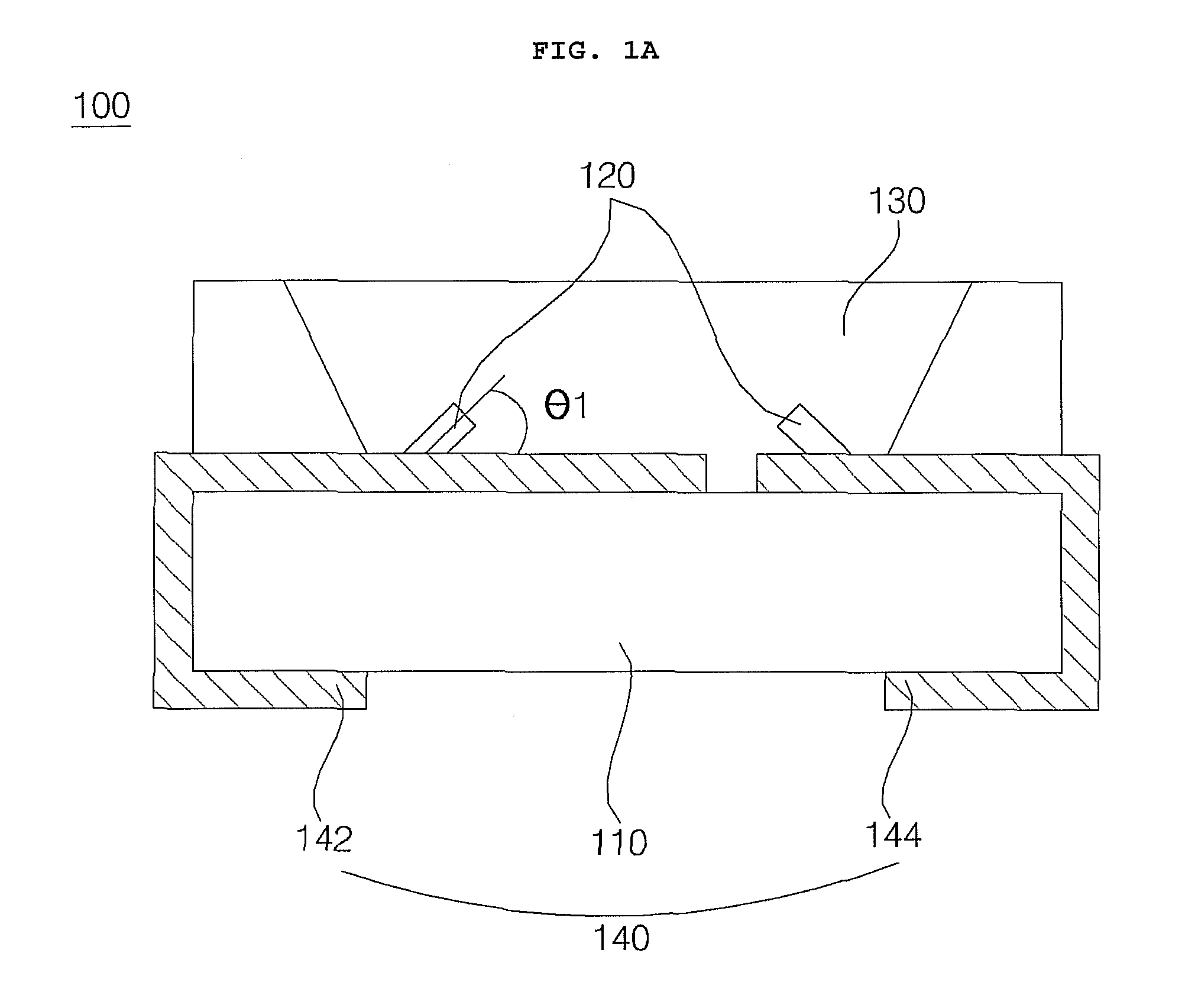
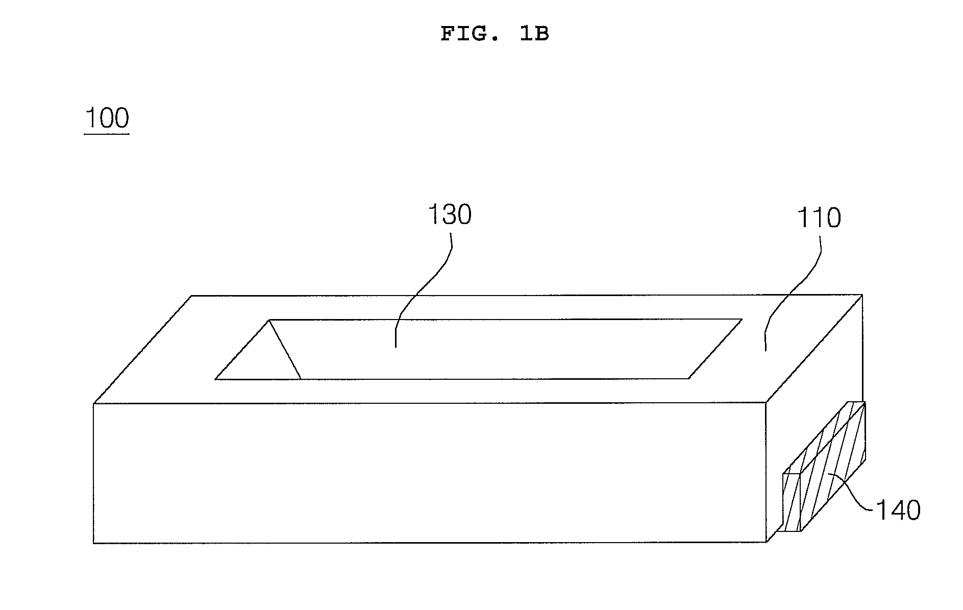
[0026]FIG. 1A is a cross-sectional view ...


PUM


Abstract

Disclosed is a light-emitting diode package according to an embodiment, including; a body having a cavity formed therein, a lead frame placed in the cavity; and a light emitting diode electrically connected to the lead frame while having a slope angle relative to the bottom surface of the cavity, wherein a light emitting part and a non-light emitting part are present on the light emitting diode, and wherein a connection part is provided in a region of the cavity to be connected to at least a region of the non-light emitting part.

Description

CROSS-REFERENCE TO RELATED APPLICATION[0001]This application claims the priority benefit of Korean Patent Application No. 10-2011-0055019, filed on Jun. 8, 2011 in the Korea Intellectual Property Office, the disclosure of which is incorporated herein by reference.BACKGROUND[0002]1. Field[0003]Embodiments relate to a light-emitting diode package.[0004]2. Description of the Related Art[0005]A light-emitting diode (LED) is a device which converts electricity into light using characteristics of compound semiconductors. LEDs are now being applied to devices such as home appliances, remote controls, electronic signboards, displays, a variety of automatic appliances and the like and their application range continues to expand.[0006]A light-emitting diode generally dissipates energy, in particular, in heat or light form corresponding to an energy gap between a conduction band and a valence band through combination of electrons in an n-layer and holes in a p-layer by applying forward voltage...

Claims


Application Information

Patent Timeline
Patent Type & Authority Patents(United States)
IPC IPC(8): H01L33/62H01L25/075H01L33/48
CPCH01L25/0753H01L33/486H01L33/62H01L2924/0002H01L2924/00H01L27/15H01L33/483H01L33/50
Inventor LEE, SANGWOOWON, SUNGHEE
Owner SUZHOU LEKIN SEMICON CO LTD
Why Eureka
Try Eureka