

Vertical LED with conductive vias
a technology of conductive vias and leds, which is applied in the direction of semiconductor/solid-state device manufacturing, electrical apparatus, and semiconductor devices. it can solve the problems of optically lossy metal contacts in the close vicinity of light emitting heterostructure, limiting factors reducing the extraction efficiency of leds, and emitted photons being totally internally reflected. it can improve light extraction efficiency, increase scattering, and maximize light extraction
- Summary
- Abstract
- Description
- Claims
- Application Information
AI Technical Summary
Benefits of technology
Problems solved by technology
Method used
Image

Examples
first embodiment
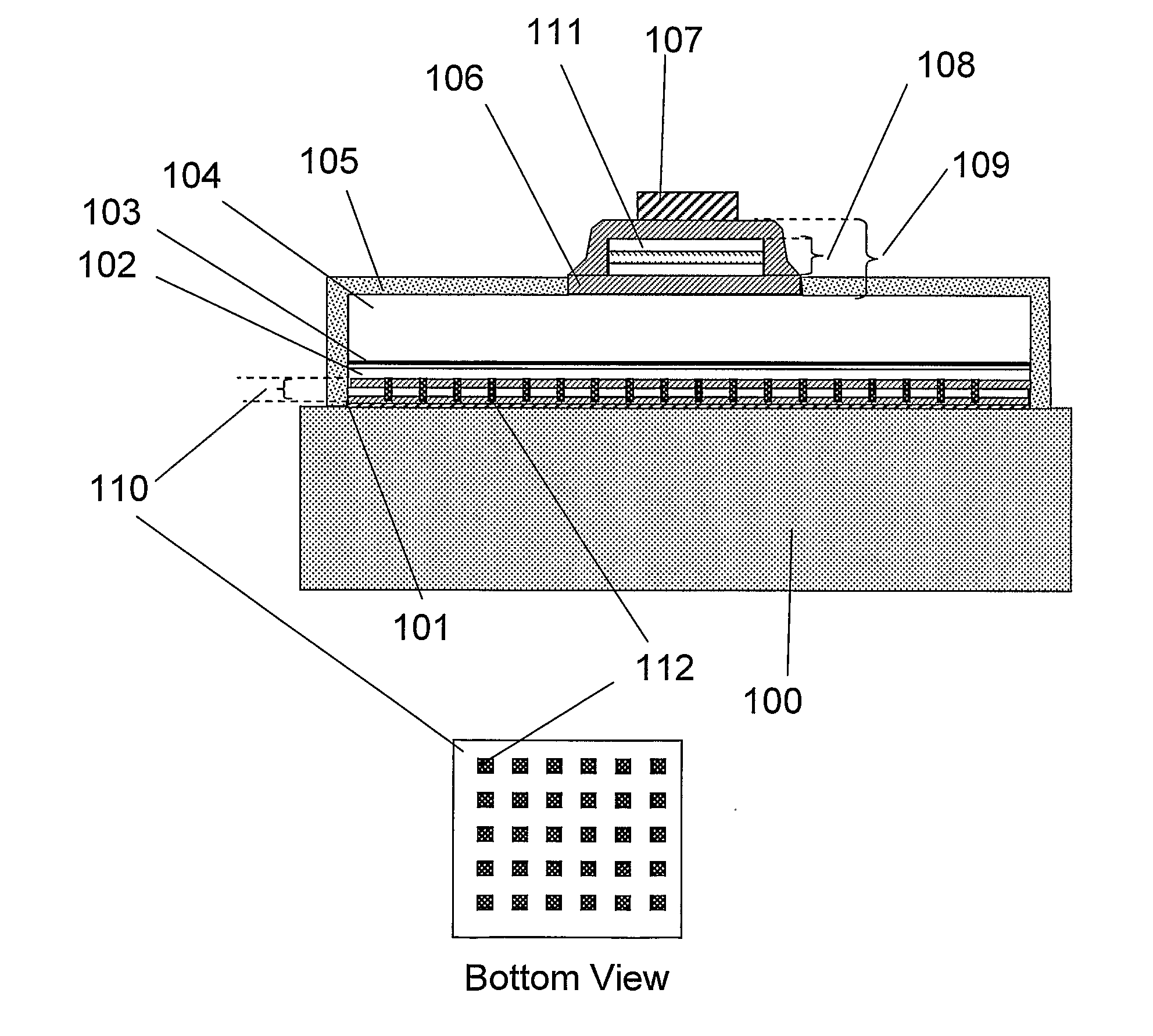
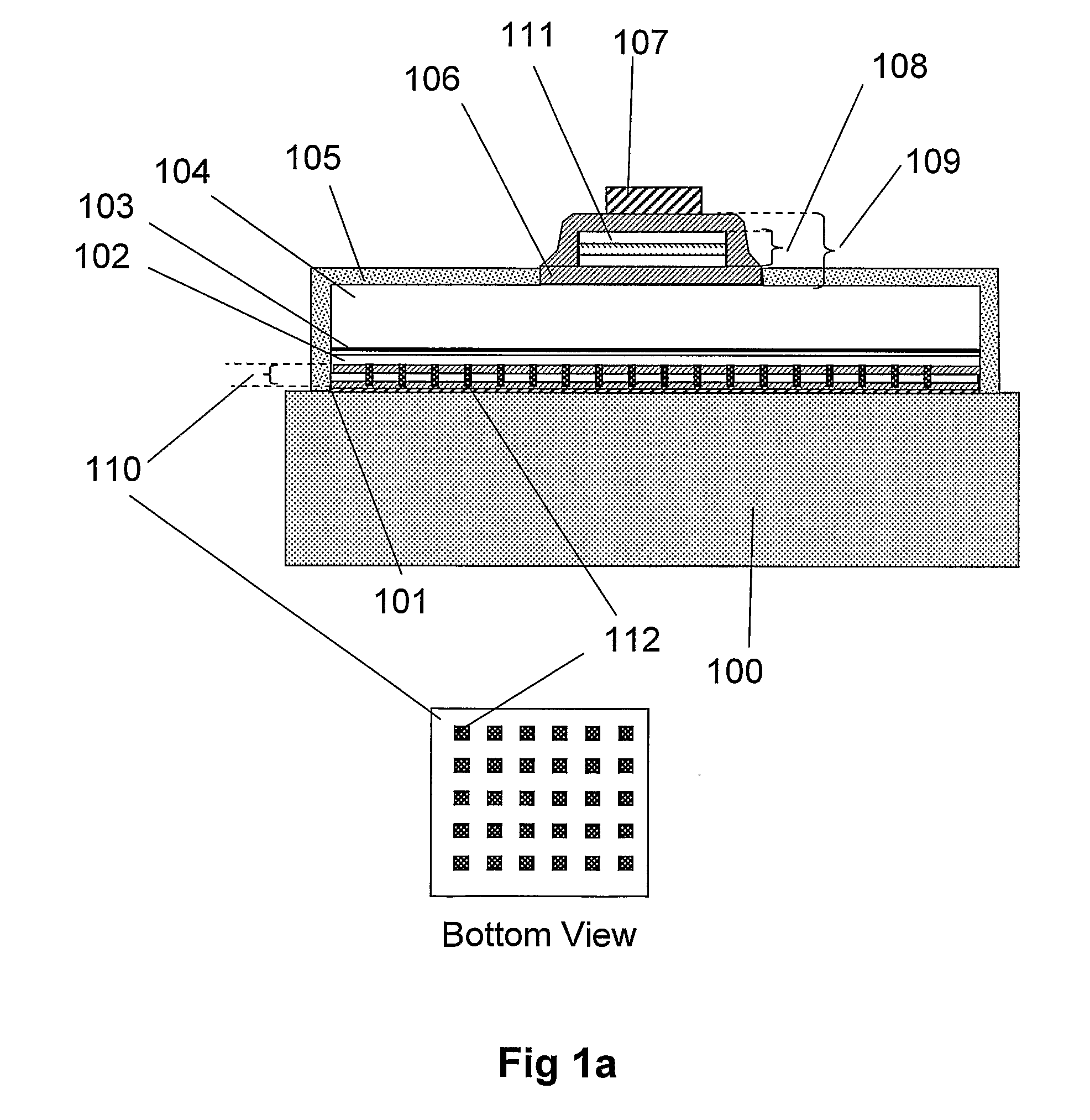
[0096]In the invention a novel low loss bottom CVMR stack, 110, is employed between the reflective metal bottom contact, 101, and the p-GaN flip chip layer, 102. This is indicated in FIG. 1. The layer 101 can also comprise a multilayer of electrical and thermal conducting metals optimised for maximal adhesion and highest optical reflectivity. Layer 101 can comprise, but is not restricted to, single or multilayers of 5 to 15 nm of Ni, Cr, Pt, Ti or Ru for adhesion, while additional multilayers of Al and Ag can be employed for improved reflectivity at wavelengths in the UV and blue region. Additionally, layers such as, but not exclusively, Cu or Ag may also be employed for improved bonding with the underlying substrate.
[0097]The layer 101 resides on top of a conductive substrate 100 which also acts as the bottom p-contact. The CVMR comprises at least 3 material layers, and can comprise 4 layers, 5 layers or more. The at least 3 material layers comprise of at least 2 different dielectr...
second embodiment
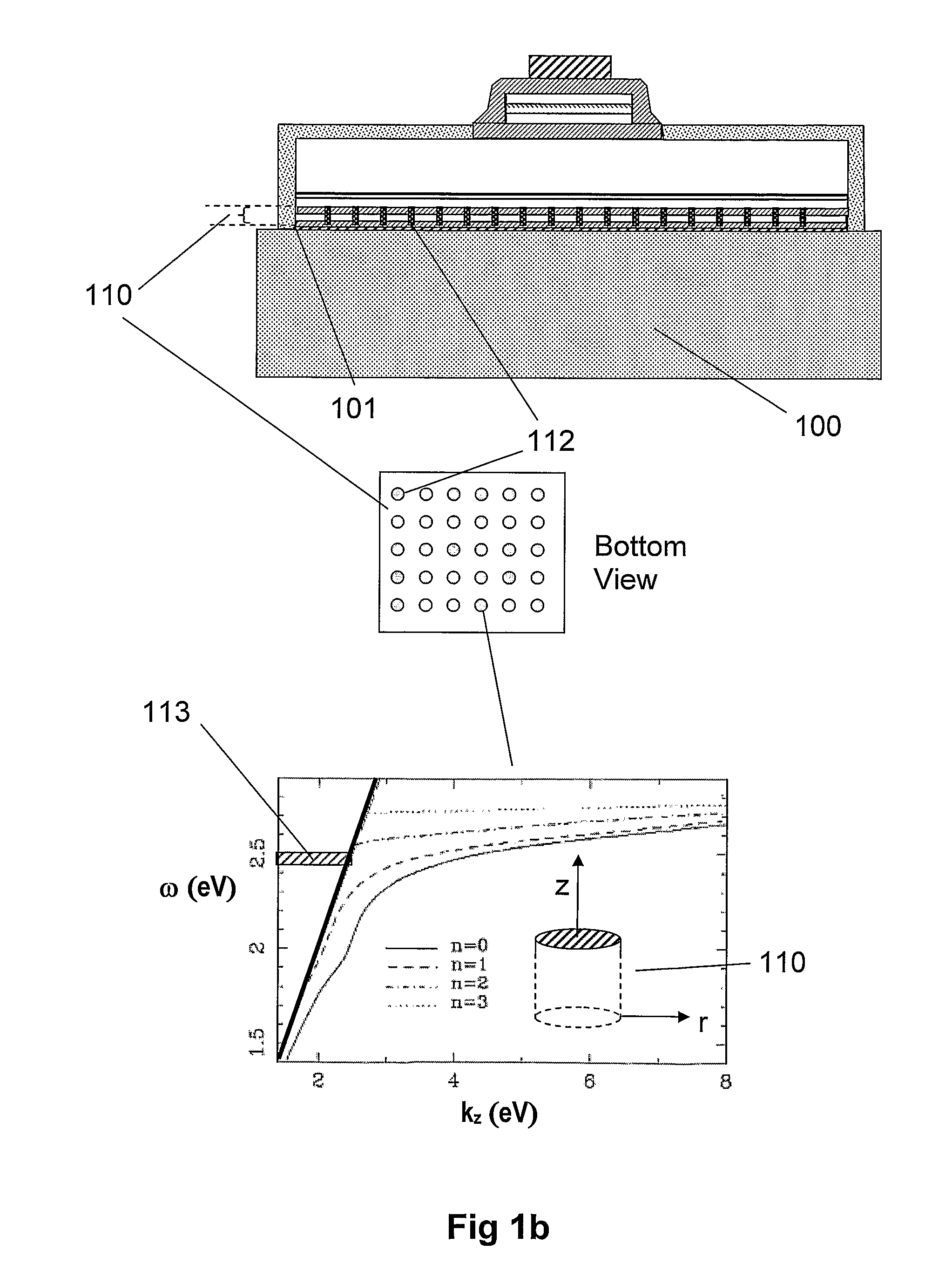
[0113]In the present invention the vias may comprise a metal shell, 115, surrounding a dielectric core, 114. In FIG. 1c an exemplary structure is highlighted. The addition of another 2 degrees of freedom, in this case the inner core radius of the dielectric medium and its refractive index, allows for greater flexibility in shifting the surface plasmon modes away from the incident wave-vectors of the LED device. By fixing the inner core (80 nm with dielectric core refractive index of approx. 2.0), and reducing the outer radius of metal+dielectric from approximately 110 nm to 100 nm, the dispersion relations shift is clearly visible as shown in FIGS. 1d and 1e, respectively.
[0114]It is also an advantage of the present invention to employ metallic cylindrical shell vias for the high speed modulation of LED devices. Recent trends in LED colour mixing involve the use of modulated Red, Green and Blue LEDs to achieve the desired colour.
[0115]Additionally, for the enabling of efficient curr...
PUM
 Abstract
Description
Claims
Application Information