Method of detecting and measuring contact alignment shift relative to gate structures in a semicondcutor device

a technology of semiconductor devices and alignment shifts, which is applied in the direction of semiconductor/solid-state device testing/measurement, electrical equipment, basic electric elements, etc., can solve the problems of performance degradation or even failure of semiconductor devices, and the requirements of precise process control may not be satisfied, so as to achieve quick and accurate detection and measurement, the effect of yield enhancemen

Active Publication Date: 2016-02-23
SHANGHAI HUALI MICROELECTRONICS CORP
View PDF4 Cites 2 Cited by
  • Summary
  • Abstract
  • Description
  • Claims
  • Application Information

AI Technical Summary

Benefits of technology

[0010]Accordingly, at least one object of the present invention is to provide an accurate detection and measurement of the alignment shifts between the contact holes and the gate structures.
[0032]The present invention provides a quick and accurate detection and measurement of the alignment shift of the contacts relative to the gate structures by designing different test model regions in which NMOS (or PMOS) transistors of different critical dimensions having contacts and gate structures are formed, scanning the test model regions through e-beam inspectors in a corresponding positive (or negative) mode to obtain light-dark patterns of the contacts, and detecting and measuring the alignment shift according to the transistor critical dimensions and the light-dark patterns. The present invention not only detects the misalignment of the contacts relative to the gate structures conveniently, but also provides reference to the online monitoring of the semiconductor device manufacturing process and ensures the yield enhancement.

Problems solved by technology

As the critical dimension has reduced below 65 nm, tiny alignment shifts between the contacts and the gate structures, for example due to mask misalignment, may cause the contacts short the gate structures to the substrate and lead to electric leakages, and may further result in performance degradation or even failure in the semiconductor device.
However, with the continuous shrinking of the device dimension, the alignment shifts may not be accurate detected through optical detecting methods due to the resolution limitation thereof, and thus the requirements of precise process control may not be satisfied.

Method used


Image

  • Method of detecting and measuring contact alignment shift relative to gate structures in a semicondcutor device
  • Method of detecting and measuring contact alignment shift relative to gate structures in a semicondcutor device
  • Method of detecting and measuring contact alignment shift relative to gate structures in a semicondcutor device

Examples


Embodiment Construction

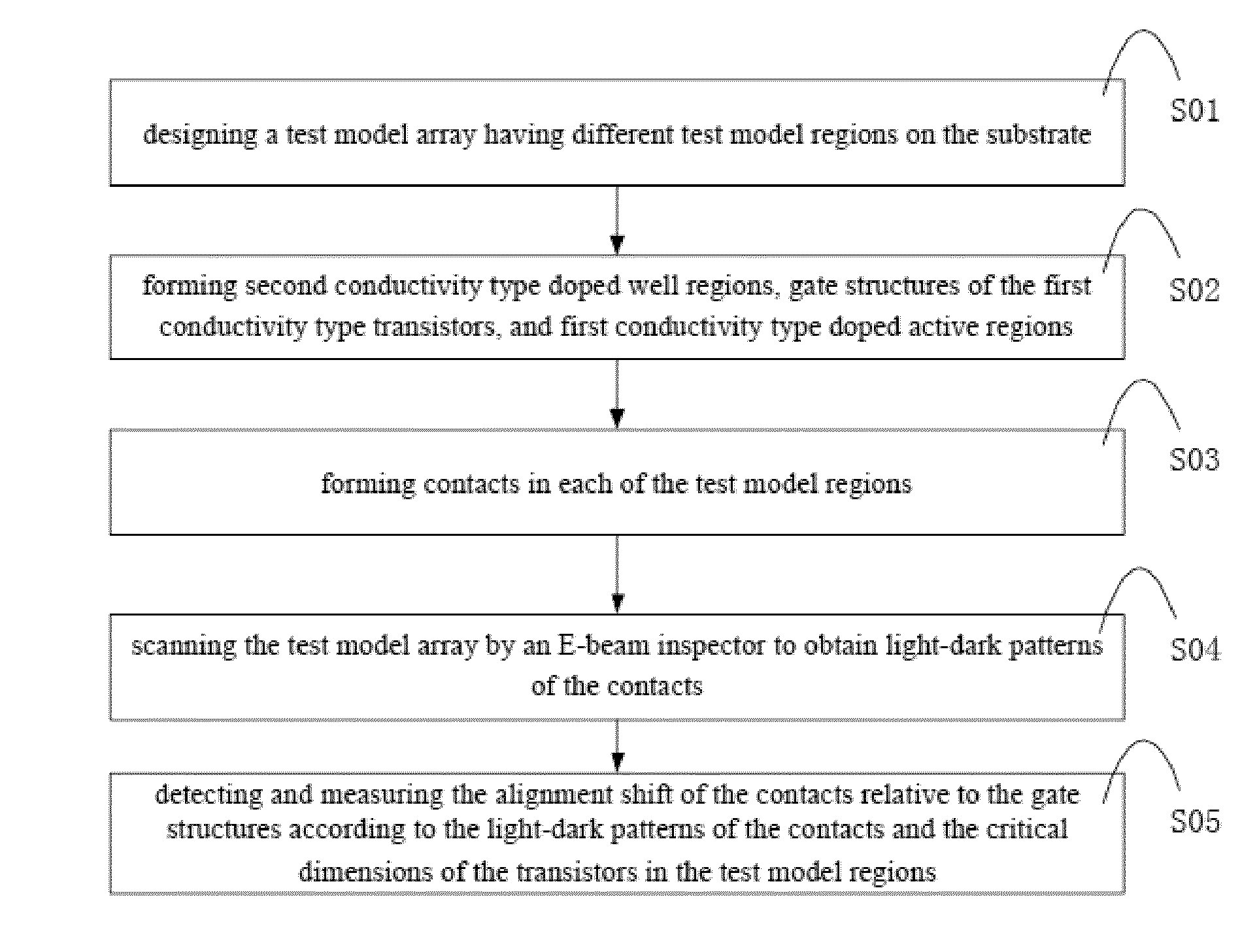
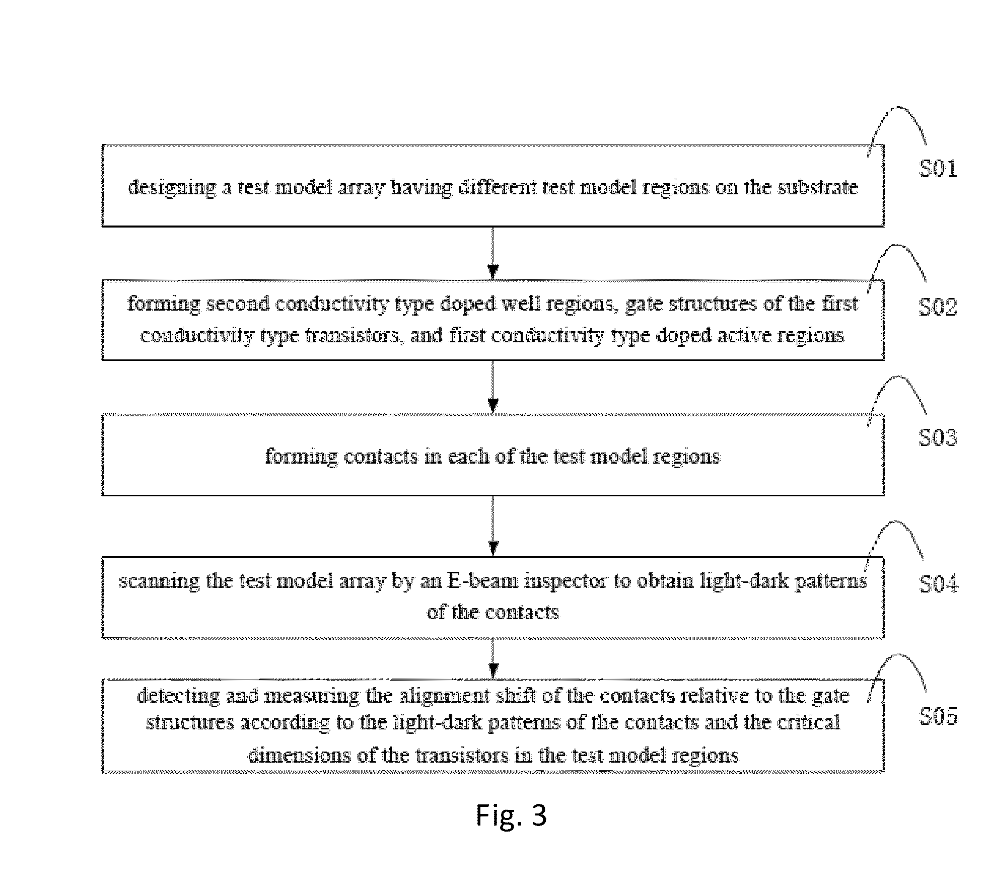
[0043]Reference will now be made in detail to the present preferred embodiments and the accompanying FIGS. 3-13 of the invention in order to provide a further understanding of the invention. The figures are not drawn to scale and they are provided merely to illustrate the invention instead of limiting the scope of the present invention, like reference numerals are used throughout the figures to designate similar or equivalent element. It should be understood that numerous specific details, relationships, and methods are set forth to provide a full understanding of the invention. One having ordinary skill in the relevant art, however, will readily recognize that the invention can be practiced without one or more of the specific details or with other methods. In other instances, well-known structures or operations are not shown in detail to avoid obscuring the invention.

[0044]Referring to FIG. 3, the method of detecting and measuring the alignment shift of the contacts relative to the...


PUM


Abstract

The present invention provides a method of detecting and measuring the alignment shift of the contacts relative to the gate structures. The method comprises: designing a test model array having different test model regions on the substrate; forming second conductivity type doped well regions, gate structures, and first conductivity type doped active regions in each of the test model regions; forming contacts in each of the test model region; scanning the test model array by an electron-beam inspector to obtain light-dark patterns of the contacts; and detecting and measuring the alignment shift of the contacts relative to the gate structures according to the light-dark patterns of the contacts and the critical dimensions of the transistors in the test model regions.

Description

CROSS-REFERENCE TO RELATED APPLICATION[0001]This application claims the priority benefit of China application serial no. 201310256841.4, filed Jun. 25, 2013. All disclosure of the China application is incorporated herein by reference.FIELD OF THE INVENTION[0002]The present invention relates to the field of semiconductor fabrication technology and particularly to a method of detecting and measuring the contact alignment shift relative to the gate structures in a semiconductor device.BACKGROUND OF THE INVENTION[0003]With the development of the IC technology and the continuous scaling down of the critical dimension, new materials and processes are introduced in the IC manufacturing process to satisfy the overall functionality of the IC products. Therefore, alignment accuracy between different structures in a semiconductor device has become more important. As the critical dimension has reduced below 65 nm, tiny alignment shifts between the contacts and the gate structures, for example d...

Claims


Application Information

Patent Timeline
Patent Type & Authority Patents(United States)
IPC IPC(8): H01L21/00H01L21/66
CPCH01L22/12H01L22/30
Inventor FAN, RONGWEILIU, FEIJUELONG, YINNI, QILIANGCHEN, HUNGLIN
Owner SHANGHAI HUALI MICROELECTRONICS CORP
Why Eureka
Try Eureka