Organic light emitting display device and method of manufacturing the same

a light-emitting display and organic technology, applied in the direction of organic semiconductor devices, semiconductor devices, electrical devices, etc., can solve the problem of deformation of the transmittance portion shape, and achieve the effect of easy patterned

Active Publication Date: 2016-03-15
SAMSUNG DISPLAY CO LTD
View PDF27 Cites 28 Cited by
  • Summary
  • Abstract
  • Description
  • Claims
  • Application Information

AI Technical Summary

Benefits of technology

[0008]The present invention also provides an organic light emitting display device in which a cathode is easily patterned and a method of manufacturing the organic light emitting display device.

Problems solved by technology

However, due to a process in which cathodes are deposited while the fine metal mask is moved several times, a position error with respect to formation of the transmittance portion occurs, and a shape of the transmittance portion is deformed.

Method used


Image

  • Organic light emitting display device and method of manufacturing the same
  • Organic light emitting display device and method of manufacturing the same
  • Organic light emitting display device and method of manufacturing the same

Examples


Embodiment Construction

[0027]Hereinafter, the present invention will be described in detail by explaining exemplary embodiments of the invention with reference to the attached drawings. Throughout the specification, a term “and / or” includes at least one from among all listed components and one or more combinations of all listed components.

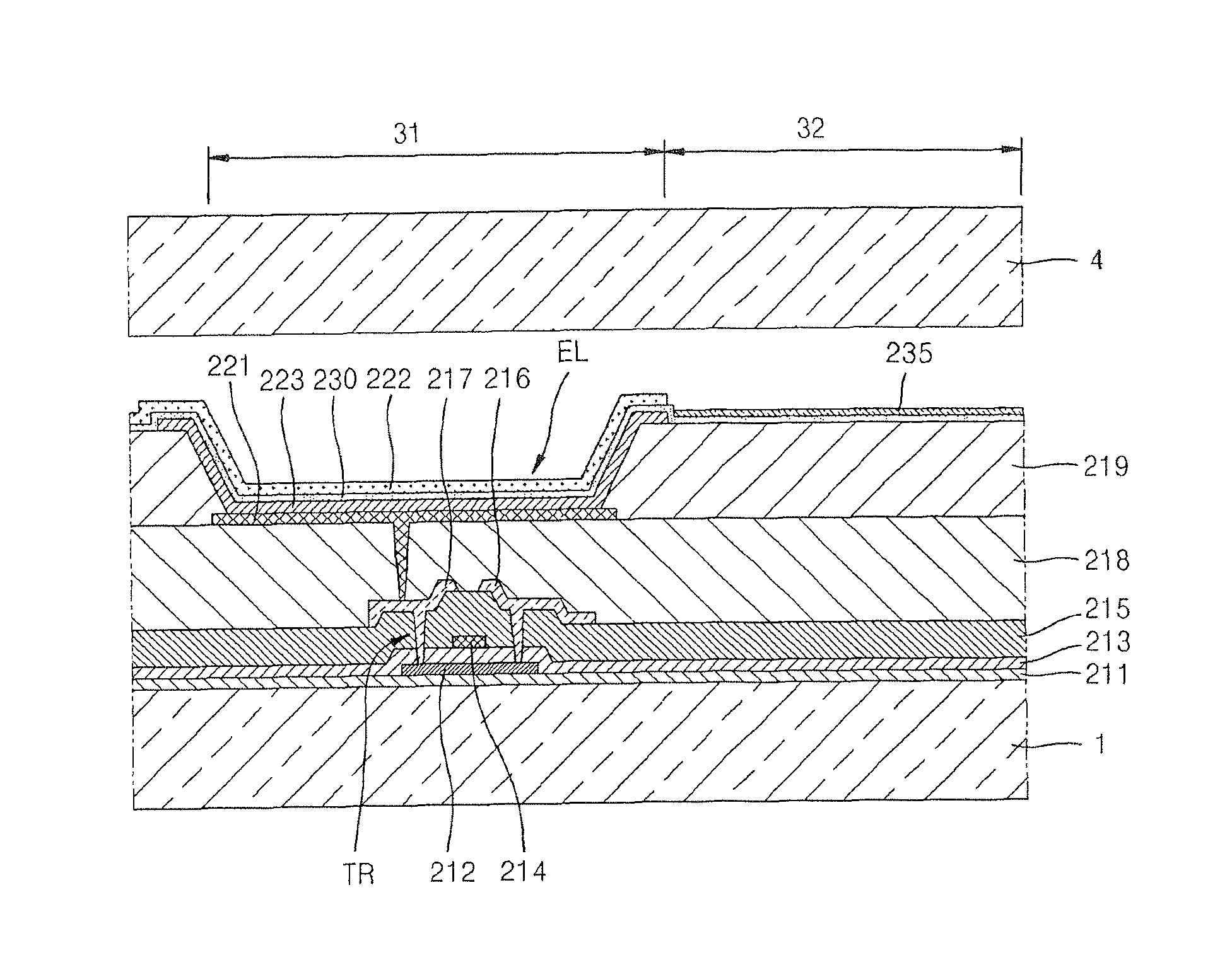
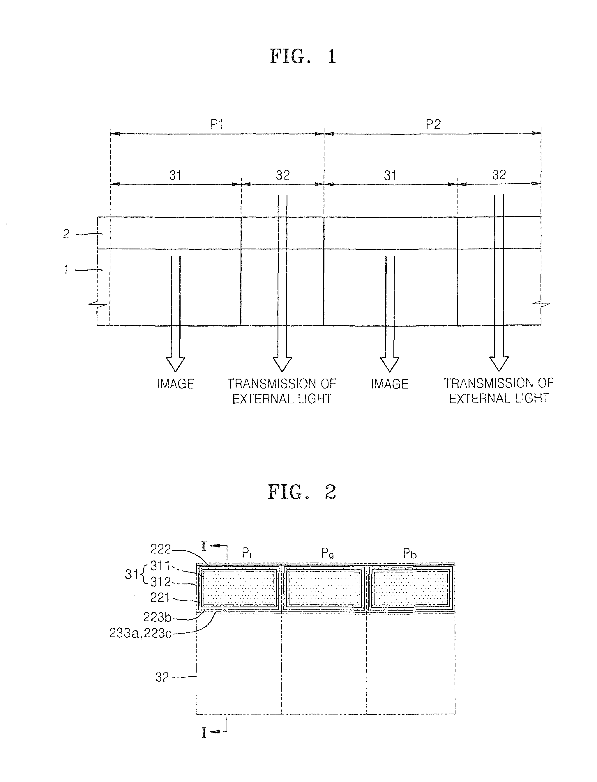
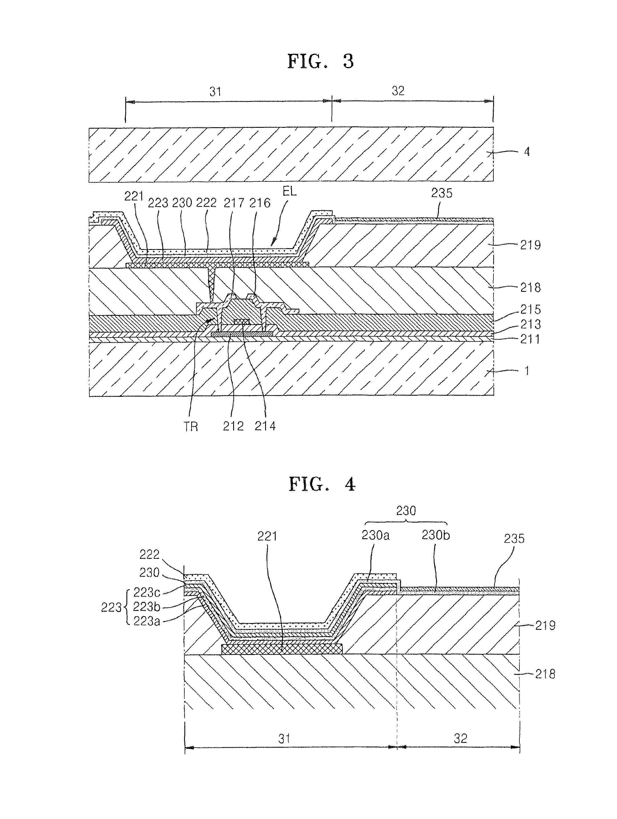
[0028]Turning now to FIG. 1, FIG. 1 illustrates a first pixel P1 and a second pixel P2, which are two neighboring pixels of an organic light emitting display device. FIG. 1 also shows a cross-sectional view of the organic light emitting display device. Referring to FIG. 1, the organic light emitting display device has a structure in which a display unit 2 is arranged on a substrate 1. In the organic light emitting display device, external light is incident by passing through the substrate 1 and the display unit 2.

[0029]As will be described later, the display unit 2 is formed to be transparent with respect to external light, so that, in FIG. 1, a user positioned at a side...


PUM


Abstract

An organic light emitting display and a method of manufacturing the same. The organic light-emitting display is a transparent display where one can see through the display to view an image on the other side of the display. Each pixel of the display has a first region that includes an organic light emitting diode and a thin film transistor, and a larger second region that is transparent. The second region is made of either transparent layers or ultra thin layers so that light is not blocked. A second electrode of the display may include magnesium and may be produced by a selective deposition process, so that use of a fine metal mask may be avoided.

Description

CLAIM OF PRIORITY[0001]This application makes reference to, incorporates the same herein, and claims all benefits accruing under 35 U.S.C.§119 from applications for ORGANIC LIGHT EMITTING DISPLAY DEVICE AND METHOD OF MANUFACTURING THE SAME earlier filed in the Korean Intellectual Property Office on 28 Oct. 2010 and there duly assigned Serial No. 10-2010-0106022 and on 31 May 2011 and there duly assigned Serial No. 10-2011-0052386.BACKGROUND OF THE INVENTION[0002]1. Field of the Invention[0003]The present invention relates to an organic light emitting display device and a method of manufacturing the same, and more particularly, to a transparent organic light emitting display device and a method of manufacturing the same.[0004]2. Description of the Related Art[0005]An organic light emitting display device is widely used in personal portable devices including MPEG-1 Audio Layer-3 (MP3) players and mobile phones, televisions (TVs), and the like due to its wide viewing angle, high contra...

Claims


Application Information

Patent Timeline
Patent Type & Authority Patents(United States)
IPC IPC(8): H01L29/18H01L33/00H01L27/32H01L27/12H01L51/52
CPCH01L27/326H01L51/5221H01L27/1225H01L51/5234H01L2227/323H01L2251/5323H10K59/121H10K50/82H10K50/828H10K2102/3031H10K59/1201H10K59/1213H10K50/81H10K50/824H10K2102/00H10K2102/351
Inventor LEE, JOO-HYEONPARK, BYOUNG-HEECHUNG, JIN-KOOCHOI, JUN-HOKIM, SEONG-MIN
Owner SAMSUNG DISPLAY CO LTD
Why Eureka
Try Eureka