Solder, microelectromechanical component and device, and a process for producing a component or device

Inactive Publication Date: 2008-07-22
NAVAJO MFG +1
View PDF15 Cites 15 Cited by
  • Summary
  • Abstract
  • Description
  • Claims
  • Application Information

AI Technical Summary

Benefits of technology

[0026]It is advantageous for at least one layer of the soldered joint to be applied using a thin-film

Problems solved by technology

One drawback of the gold-tin solder material is that this material, for use in thin-film technologies, for example in the case of sputtered contacts, has to be produced as a special target having approximately the same overall composition as the eutectic alloy.
It is known that the composition of multicomponent targets changes over the course of time as a result of preferential sputtering of different elements, and consequently the basic problem of a change in the composition of t

Method used


Image

  • Solder, microelectromechanical component and device, and a process for producing a component or device
  • Solder, microelectromechanical component and device, and a process for producing a component or device
  • Solder, microelectromechanical component and device, and a process for producing a component or device

Examples


Embodiment Construction

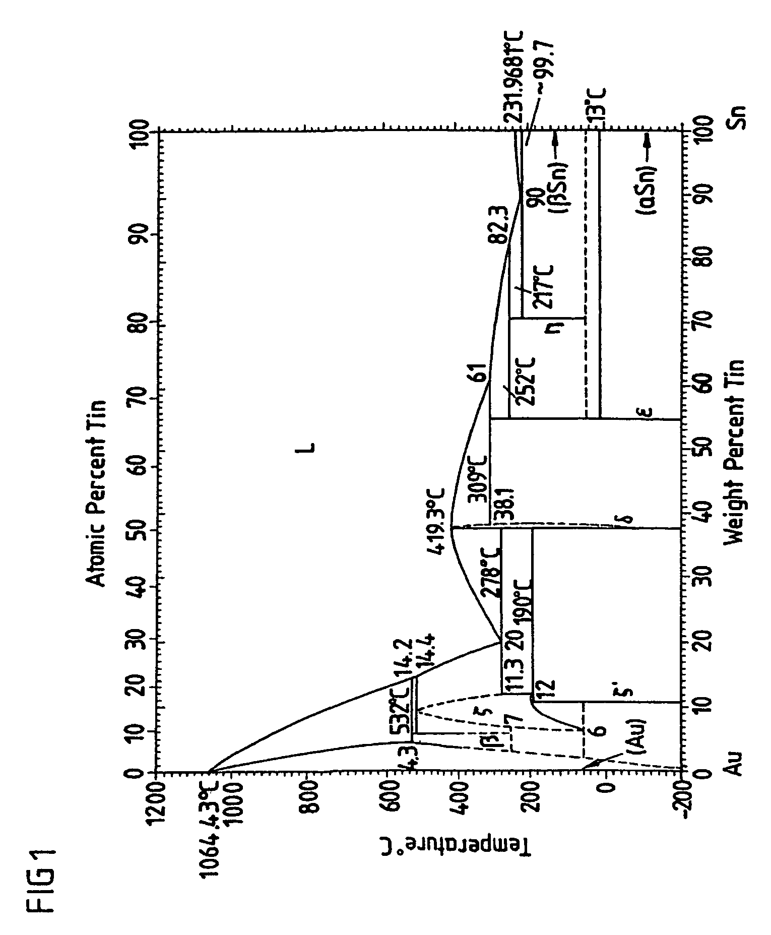
[0040]FIG. 1 illustrates a phase diagram for the binary gold-tin (AuSn) system, which is used as thin-film solder in the electronics industry.

[0041]The eutectic at 30 atomic % tin, 70 atomic % Au (upper x axis) is of relevance to the present invention.

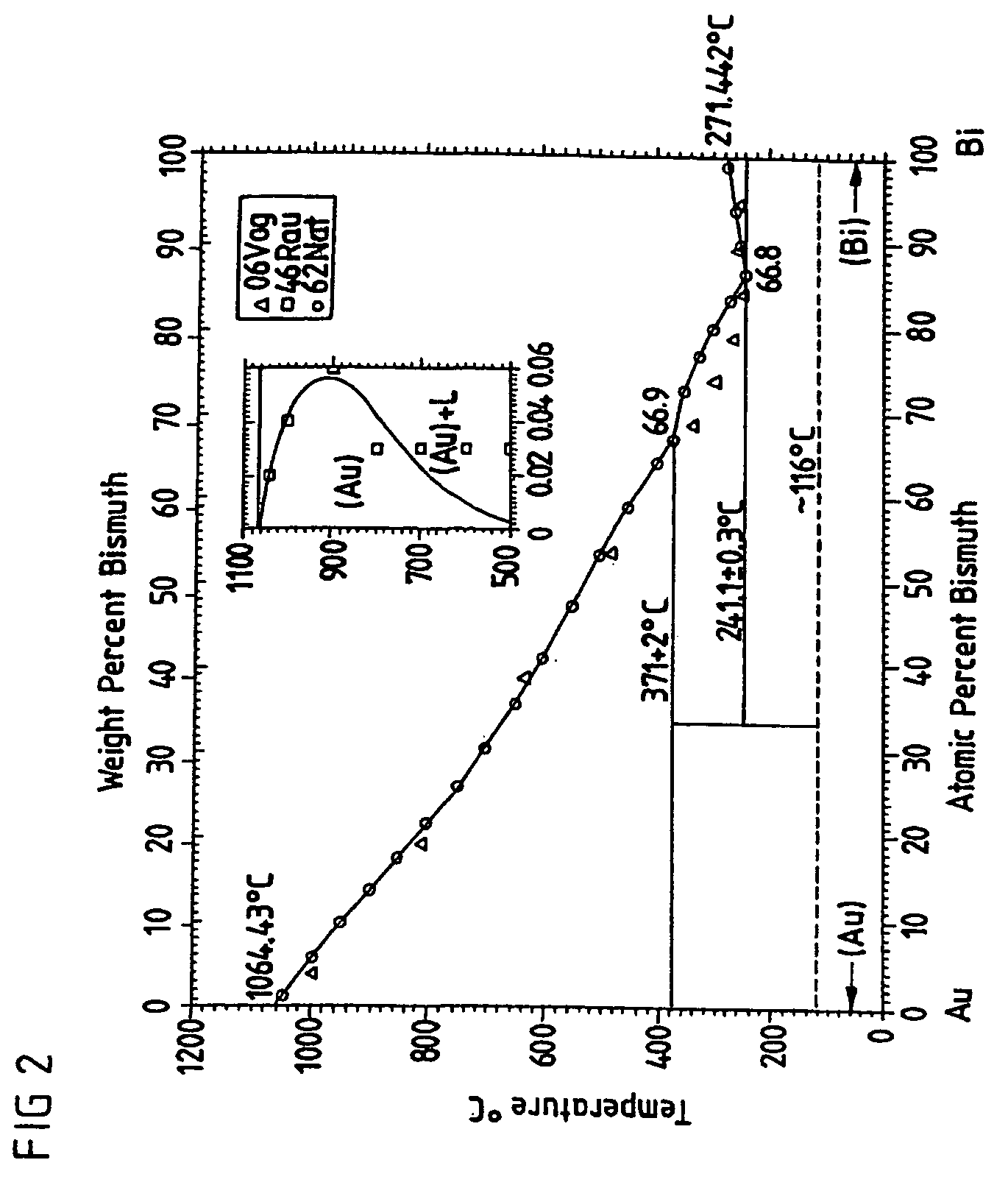
[0042]FIG. 2 shows a phase diagram for an embodiment of the thin-film solder according to the invention with a gold-bismuth (AuBi) system. The atomic percentages of bismuth are plotted on the lower x axis. This materials system has the required low eutectic temperature, namely 241° C. at approx. 87 atomic % of bismuth. The solidus curve rises only slowly, starting from the eutectic point, i.e. the temperature of the final melt is less sensitive to minor fluctuations in concentration.

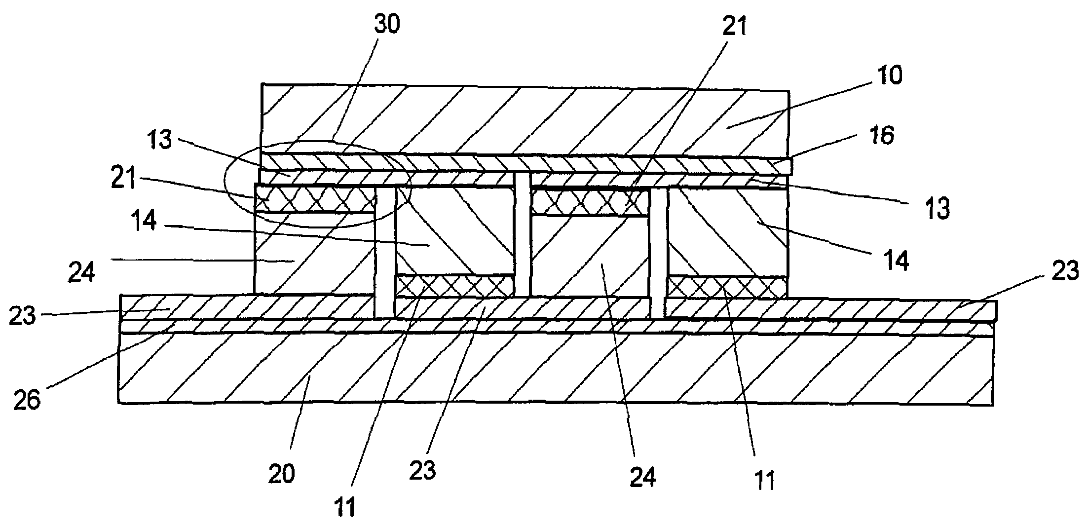
[0043]For the production of thin-film thermoelectric devices, as in DE 198 45 104 A1, the fabrication sequence described in that document is considerably simplified when a gold-bismuth system is used. The soldering partner bismuth, unlike the soldering part...


PUM

PropertyMeasurementUnit
Thicknessaaaaaaaaaa
Thicknessaaaaaaaaaa
Thermal propertiesaaaaaaaaaa

Abstract

A solder, in particular a thin-film solder, for joining microelectromechanical components, wherein the solder is a eutectic mixture of gold and bismuth. Components and devices joined by a solder of this type are also disclosed, in addition to processes for producing such components or devices.

Description

FIELD OF THE INVENTION[0001]The invention relates to a solder for joining microelectromechanical components, to a microelectronical and / or microelectromechanical component formed using this solder, to a microelectromechanical device formed using this solder, and to a process for producing a component or device using this solder.BACKGROUND OF THE INVENTION[0002]Laid-open specification DE 19 845 104 A1 describes a process for producing a microelectromechanical device, namely a thermoelectric transducer, produced in various embodiments at wafer level. In some embodiments, the thermoelectric components are assembled from two substrate wafers, coated with the respective complementary n / p materials, to form a component.[0003]The microelectromechanical device (in this case a transducer) is composed of a plurality of components. It is then possible for further components (e.g. a laser diode) to be arranged on the component.[0004]During fabrication of the thermoelectric transducer, in the fi...

Claims


Application Information

Patent Timeline
IPC IPC(8): H01L23/48H01L23/52H01L29/40B23K35/02B23K35/26B81C3/00H01L23/38H01L23/488
CPCB23K35/264B81C3/001H01L23/38H01L23/488B23K35/0238H01L2924/0002H01L2924/00
Inventor BOTTNER, HARALDSCHUBERT, AXELJAEGLE, MARTIN
Owner NAVAJO MFG
Why Eureka
Try Eureka