Transperent Conductive Substrate and Method of Manufacturing the same Touch Screen Using the Same

a technology of transparent conductive substrate and touch screen, which is applied in the direction of dielectric characteristics, instruments, transportation and packaging, etc., can solve the problem of difficult patterning of ito electrode b, and achieve the effect of preventing malfunction of touch screen and easy patterning of transparent electrod

Inactive Publication Date: 2011-11-17
SAMSUNG ELECTRO MECHANICS CO LTD
View PDF3 Cites 13 Cited by
  • Summary
  • Abstract
  • Description
  • Claims
  • Application Information

AI Technical Summary

Benefits of technology

The present invention has been made in an effort to provide a transparent conductive substrate that easily patterns a transparent electrode and prevents malfunction of a touch screen, etc. by completely removing residues, a method of manufacturing the same, and a touch screen using the same.

Problems solved by technology

However, even though the transparent conductive substrate 10 according to the prior art is formed with the primer 12 to improve the adhesion between the transparent substrate 11 and the ITO electrode 13, the primer 12 is formed over the transparent substrate 11 does not have a difference in surface characteristics, such that it is difficult to pattern the ITO electrode 13.

Method used


Image

  • Transperent Conductive Substrate and Method of Manufacturing the same Touch Screen Using the Same
  • Transperent Conductive Substrate and Method of Manufacturing the same Touch Screen Using the Same
  • Transperent Conductive Substrate and Method of Manufacturing the same Touch Screen Using the Same

Examples


first embodiment

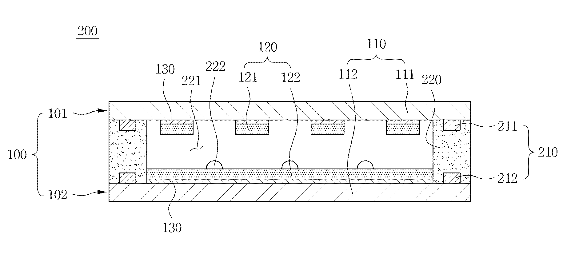
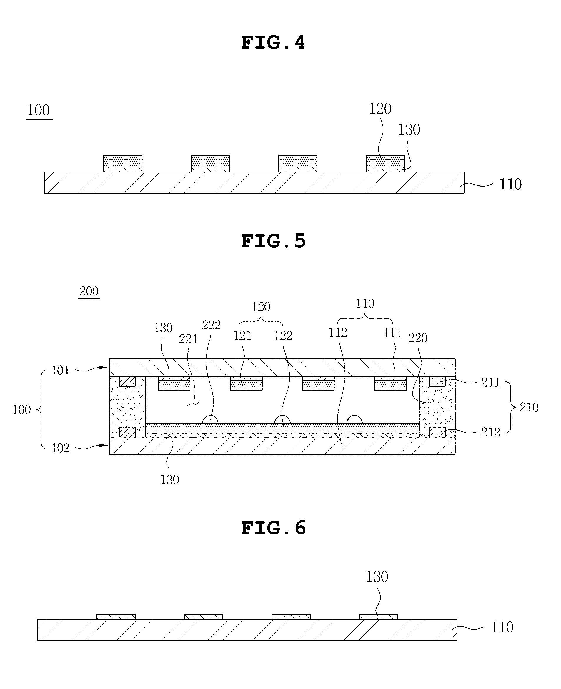
The transparent conductive substrate 100a according to the preferred first embodiment of the present invention, as shown in FIG. 8, is manufactured by the manufacturing processes as described above.

Meanwhile, even though the present embodiment describes a screen printing method as the method of manufacturing the transparent electrode 120 by way of example, the present invention is not limited thereto but may form the transparent electrode 120 by, for example, a printing method such as an inkjet printing method, a gravure printing method, an offset printing method, or the like, and a coating method.

FIGS. 9 to 11 are diagrams explaining a method of manufacturing a transparent conductive substrate 100b according to a second preferred embodiment of the present invention. Hereinafter, a method of manufacturing a transparent conductive substrate 100b according to the present embodiment will be described with reference to FIGS. 9 to 11. Herein, like reference numerals will designate identi...

second embodiment

The transparent conductive substrate 100b according to the preferred second embodiment of the present invention, as shown in FIG. 11, is manufactured by the manufacturing processes as described above.

According to the present invention, the transparent conductive substrate and the method of manufacturing the same, and the touch screen using the same, provides process convenience in patterning the transparent electrode by an etching method or a laser method by patterning the primer to correspond to the transparent electrode, and does not leave residues due to the adhesion of the primer on the portion from which the transparent electrode is to be removed.

In addition, according to the present invention, when the transparent electrode is formed by a printing method or a coating method, the primer is previously patterned to correspond to the transparent electrode, thereby preventing the material of the transparent electrode from being diffused.

In addition, according to the present inventi...


PUM

PropertyMeasurementUnit
thicknessaaaaaaaaaa
thicknessaaaaaaaaaa
thicknessaaaaaaaaaa

Abstract

Disclosed herein are a transparent conductive substrate and a method of manufacturing the same, and a touch screen using the same. The transparent conductive substrate includes a transparent substrate, a transparent electrode that is formed and patterned on the transparent substrate, and a primer that is formed between the transparent substrate and the transparent electrode and is patterned to have a pattern corresponding to the transparent electrode. The transparent electrode is easily patterned by previously patterning the primer to correspond to the transparent electrode and residues do not remain on the transparent substrate.

Description

CROSS REFERENCE TO RELATED APPLICATIONThis application claims the benefit of Korean Patent Application No. 10-2010-0044986, filed on May 13, 2010, entitled “Transparent Conductive Substrate And Method Of Manufacturing The Same And Touch Screen Using The Same”, which is hereby incorporated by reference in its entirety into this application.BACKGROUND OF THE INVENTION1. Technical FieldThe present invention relates to a transparent conductive substrate and a method of manufacturing the same, and a touch screen using the same.2. Description of the Related ArtWith the continuous development in the electronic technology and the information technology fields, the relative importance of electronic devices is constantly increasing in everyday life, including a work environment. In particular, as electronic technology continuously develops, touch screens are used in portable devices that are recently reduced in size and thickness.Touch screens, devices generally installed in display devices t...

Claims


Application Information

Patent Timeline
Patent Type & Authority Applications(United States)
IPC IPC(8): G06F3/041B05D5/12H05K3/06B32B3/10
CPCG06F3/044G06F3/045G06F2203/04103H05K1/095Y10T428/24884H05K3/1216H05K2201/0108Y10T428/24868H05K3/06G06F3/0448
Inventor KIM, WOON CHUNOH, YONG SOOLEE, JONG YOUNGJIN, YONG HYUN
Owner SAMSUNG ELECTRO MECHANICS CO LTD
Why Eureka
Try Eureka