Method of removing a hard mask on a gate

Active Publication Date: 2016-11-01
UNITED MICROELECTRONICS CORP
View PDF11 Cites 5 Cited by
  • Summary
  • Abstract
  • Description
  • Claims
  • Application Information

AI Technical Summary

Benefits of technology

The patent describes a method for making a semiconductor device with two gates. The process involves two steps: first, a first gate structure is made, including a first gate, a first hard mask, and a first spacer surrounding the first gate and hard mask; and second, a second gate structure is made, including a second gate, a second hard mask, and a second spacer surrounding the second gate and hard mask. The second hard mask has a higher top surface than the first hard mask. A dielectric layer is then formed to cover both the first and second gate structures. The first spacer is removed to expose the first hard mask and the second hard mask, followed by a second dielectric layer to cover both hard masks. A second spacer is then removed to expose the second hard mask. A second dielectric layer is formed to cover both hard masks using a same removal rate. The second dielectric layer, the first mask layer, and the second mask layer are then removed. The technical effect of this invention is to provide a method for making a semiconductor device with two gates that allows for easier and more precise control over the position of the gates during the manufacturing process. This can help to improve the reliability and performance of the semiconductor device.

Problems solved by technology

The performance of an electrical device is affected by the size of various features in the device, as well as the device switching speed and power consumption.
There are challenges, however, to implementing such features and processes in conventional fabrication.
Differences in topography of the substrate or differences in the pattern densities may cause the cap layer to be removed unevenly, so that some polysilicon gate electrodes are exposed while others are still covered by the cap layer.
The exposed polysilicon gate electrodes will have a lower height than the polysilicon gate electrodes still covered by the cap layer, making them susceptible to damage from subsequent processes.

Method used


Image

  • Method of removing a hard mask on a gate
  • Method of removing a hard mask on a gate
  • Method of removing a hard mask on a gate

Examples


Embodiment Construction

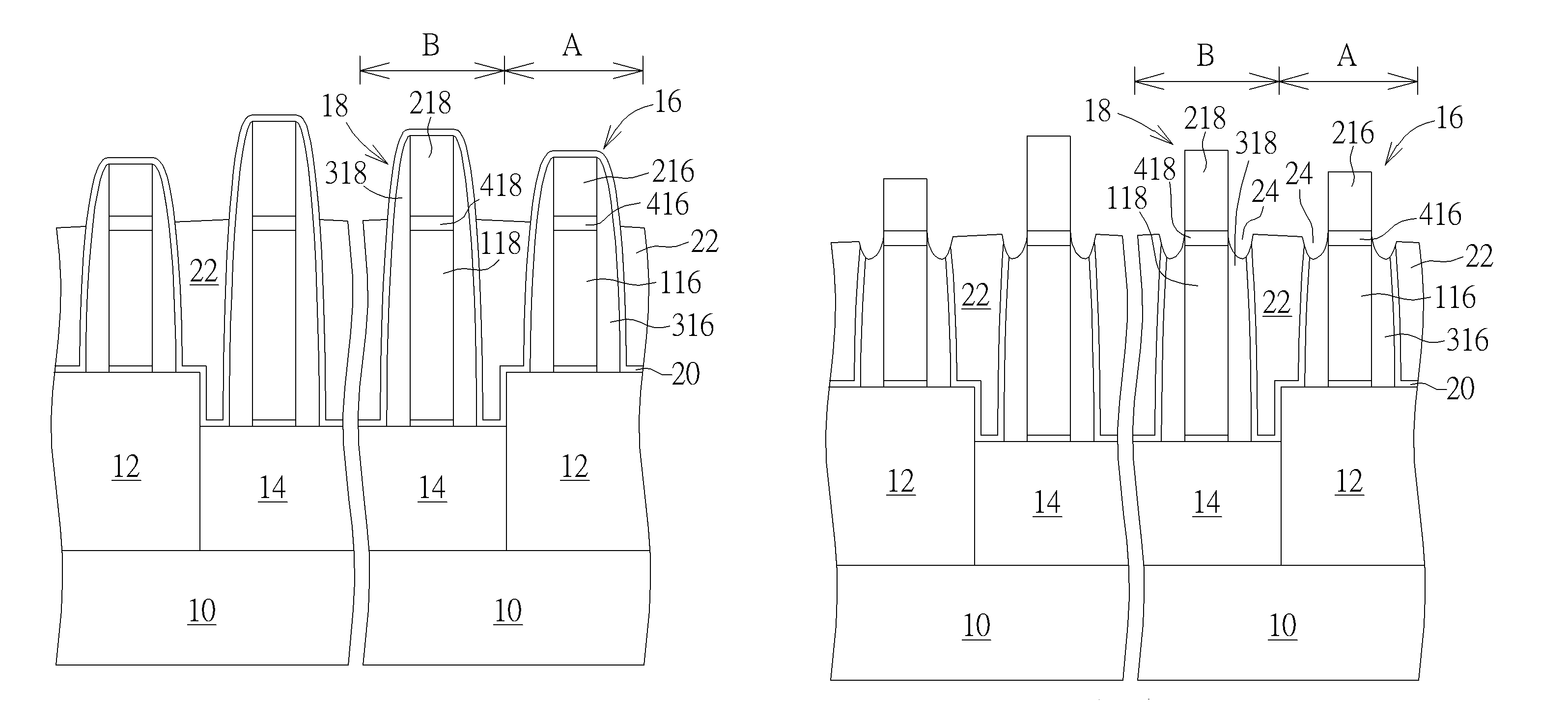
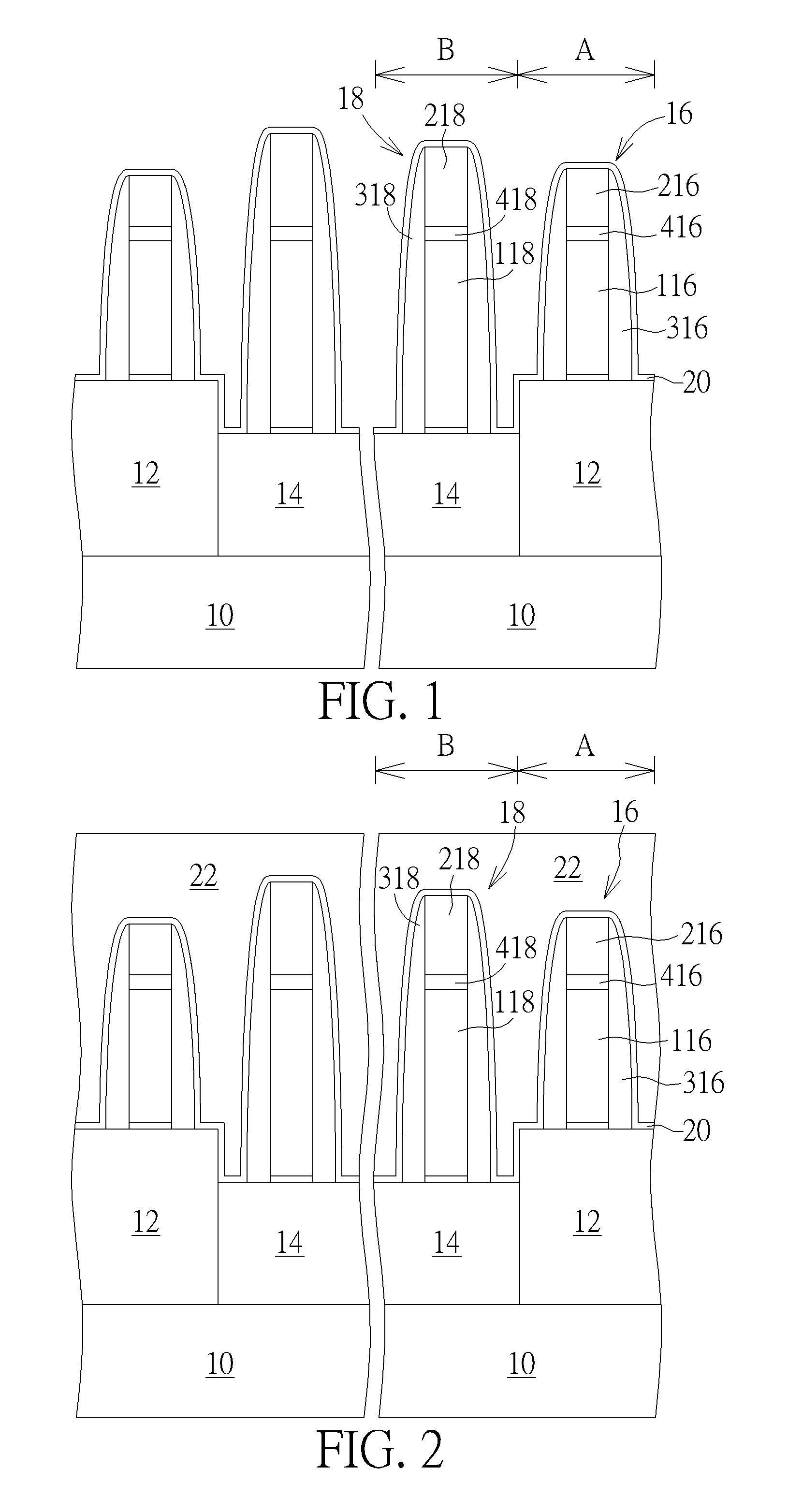
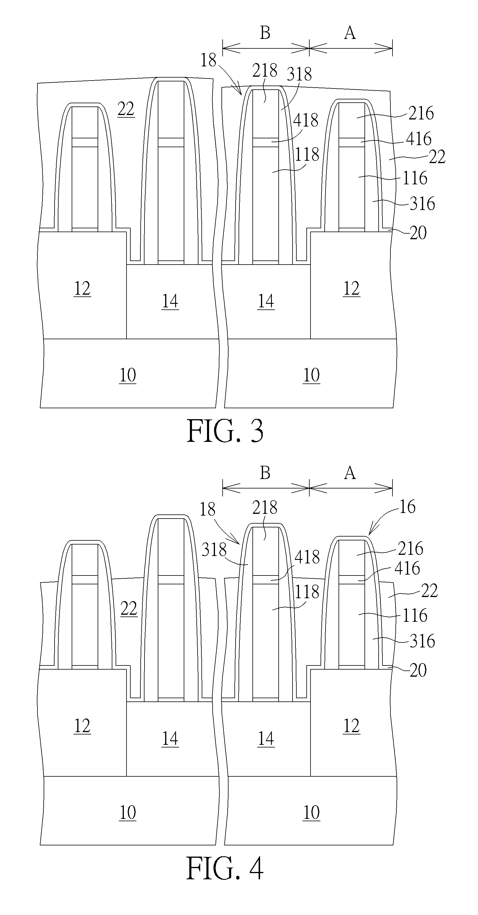
[0011]FIG. 1 to FIG. 8 depict schematically a method of removing a hard mask on a gate according to a preferred embodiment of the present invention.

[0012]As shown in FIG. 1, a substrate 10 is provided. The substrate 10 is divided into a first region A and a second region B. The first region A may include a first fin or a first STI and the second region B may include a second fin or a second STI. FIG. 1 takes the first region A including a first fin 12 and the second region B including a second STI 14 as an example. The first fin 12 protrudes from the second STI 14. A first gate structure 16 is formed on the substrate 10 within the first region A. A second gate structure 18 is formed on the substrate 10 within the second region B. In this embodiment, only two gate structures are formed; however, there can be more than two gate structures formed within the first region A or the second region B. The first gate structure 16 includes a first gate 116, a first hard mask 216 disposed on th...


PUM


Abstract

A method of removing a hard mask on a gate includes forming a first gate structure and a second gate structure. The first gate structure includes a first gate, a first hard mask disposed on the first gate and a first spacer surrounding the first gate and the first hard mask, wherein the second gate structure includes a second gate, a second hard mask disposed on the second gate and a second spacer surrounding the second gate and the second hard mask. Later, the first spacer surrounding the first hard mask and the second spacer surrounding the second hard mask are removed. After that, a dielectric layer is formed to cover the first hard mask and the second hard mask. Finally, the second dielectric layer, the first mask layer and the second mask layer are removed.

Description

BACKGROUND OF THE INVENTION[0001]1. Field of the Invention[0002]The present invention relates to a method of removing hard masks on gates, and more particularly, to a method of uniformly removing hard masks on gates.[0003]2. Description of the Prior Art[0004]The performance of an electrical device is affected by the size of various features in the device, as well as the device switching speed and power consumption. As semiconductor devices continue to decrease in size, there is a desire to replace a conventional polysilicon gate electrode with a metal gate electrode to further improve device performance. There are challenges, however, to implementing such features and processes in conventional fabrication.[0005]Before the polysilicon gate electrode can be replaced, a cap layer on top of the polysilicon gate electrode must be removed. Differences in topography of the substrate or differences in the pattern densities may cause the cap layer to be removed unevenly, so that some polysil...

Claims


Application Information

Patent Timeline
IPC IPC(8): H01L21/8234H01L21/02H01L21/3213H01L21/3105H01L29/66H01L21/28H01L21/311H01L29/06
CPCH01L21/823437H01L21/823468H01L29/6653H01L21/31055H01L21/02164H01L21/32139H01L21/0217H01L21/28035H01L21/823431H01L29/0649H01L21/31144H01L29/66545H01L21/31053H01L21/823456
Inventor LIN, CHAO-HUNGFENG, LI-WEITSAI, SHIH-HUNGJENQ, JYH-SHYANGLIN, CHING-LINGCHEN, YI-WENHUANG, CHEN-MING
Owner UNITED MICROELECTRONICS CORP
Why Eureka
Try Eureka