Anisotropic conductive adhesive, light emitting device, and method for producing anisotropic conductive adhesive
a technology of anisotropic conductive adhesive and anisotropic conductive adhesive, which is applied in the direction of vacuum evaporation coating, semiconductor/solid-state device details, coatings, etc., can solve the problems of low light emission efficiency, and difficult to improve production efficiency. , to achieve the effect of high anti-migration properties, high reflectance and high light reliability
- Summary
- Abstract
- Description
- Claims
- Application Information
AI Technical Summary
Benefits of technology
Problems solved by technology
Method used
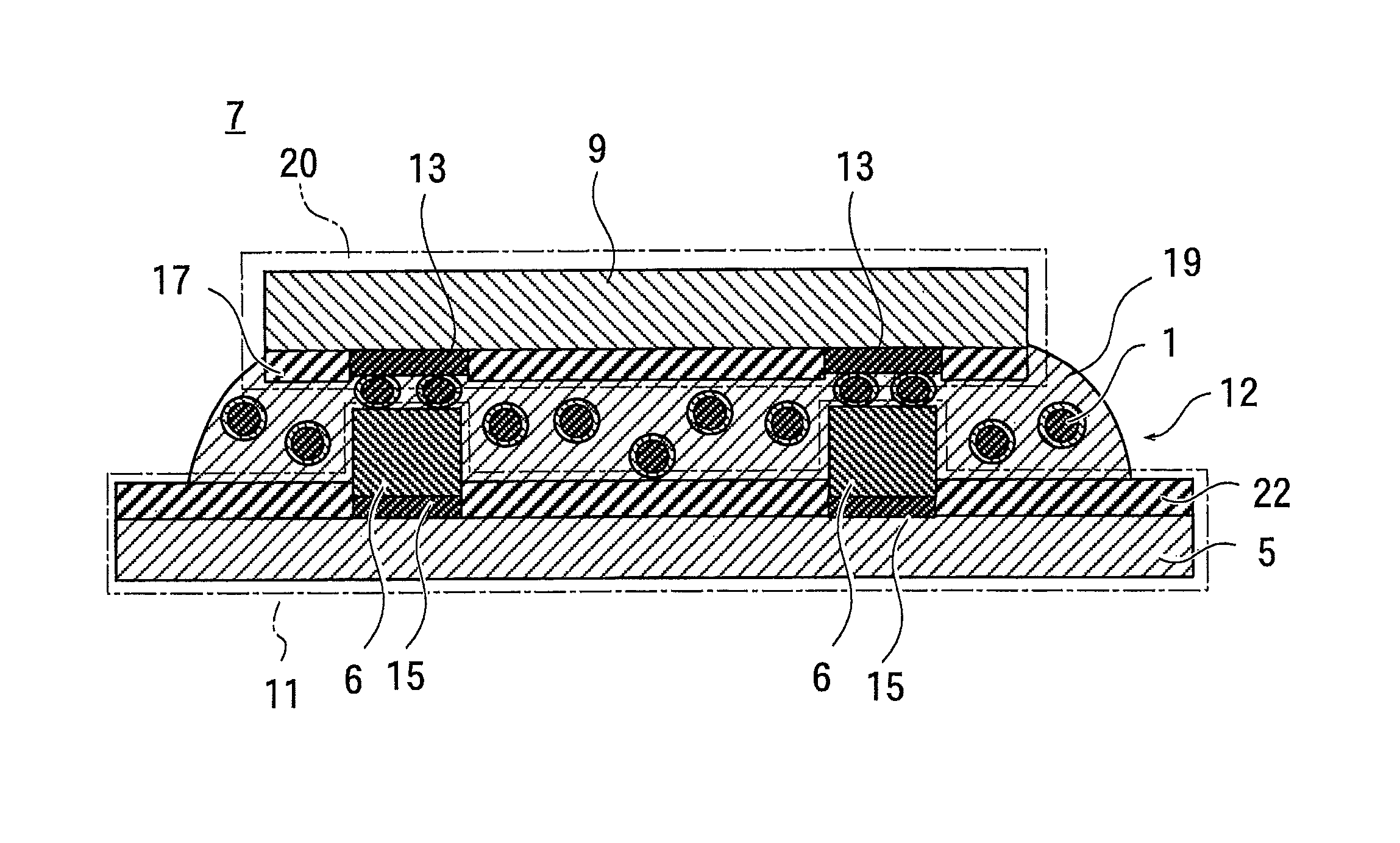
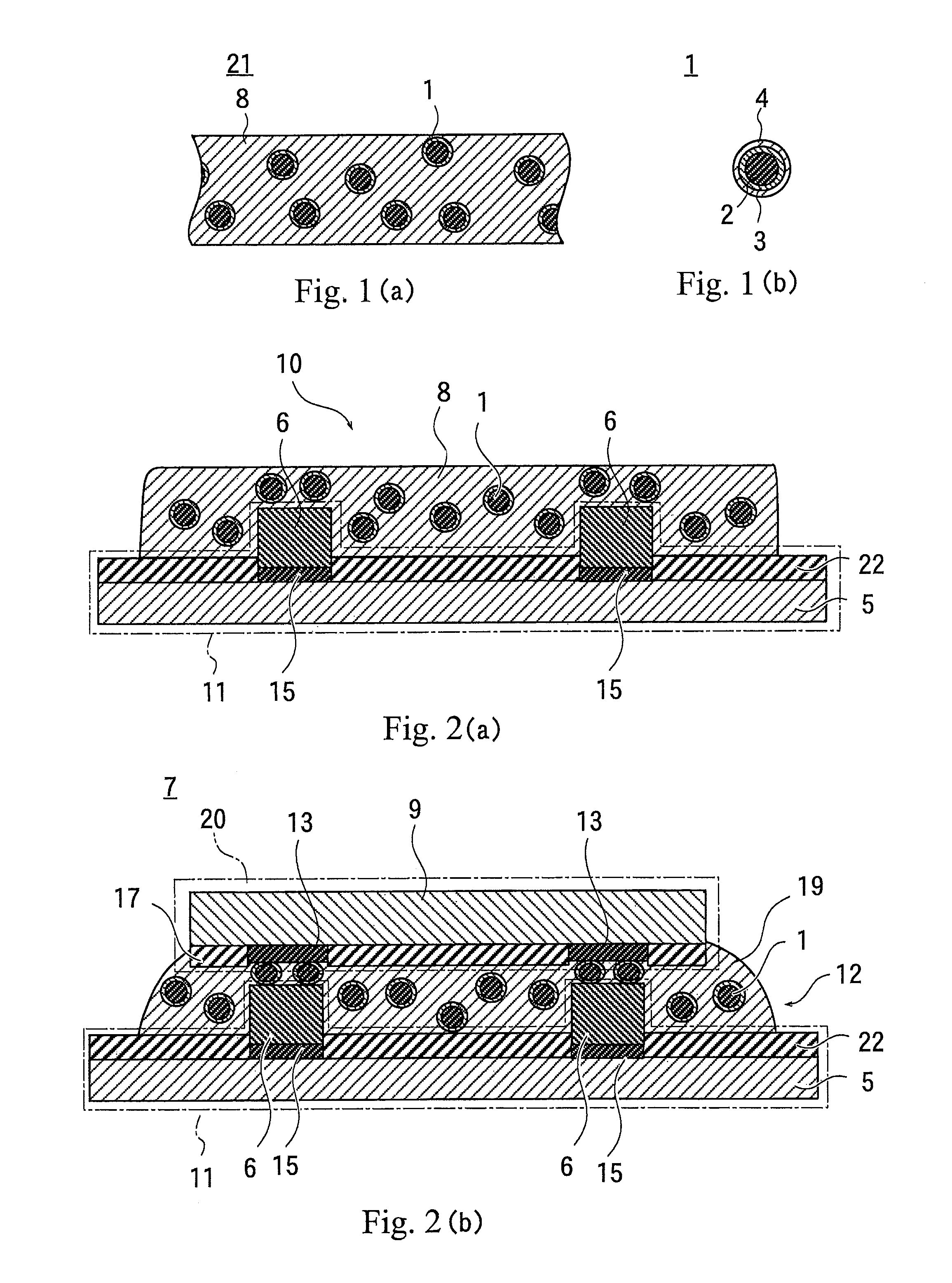
Image

Examples
examples
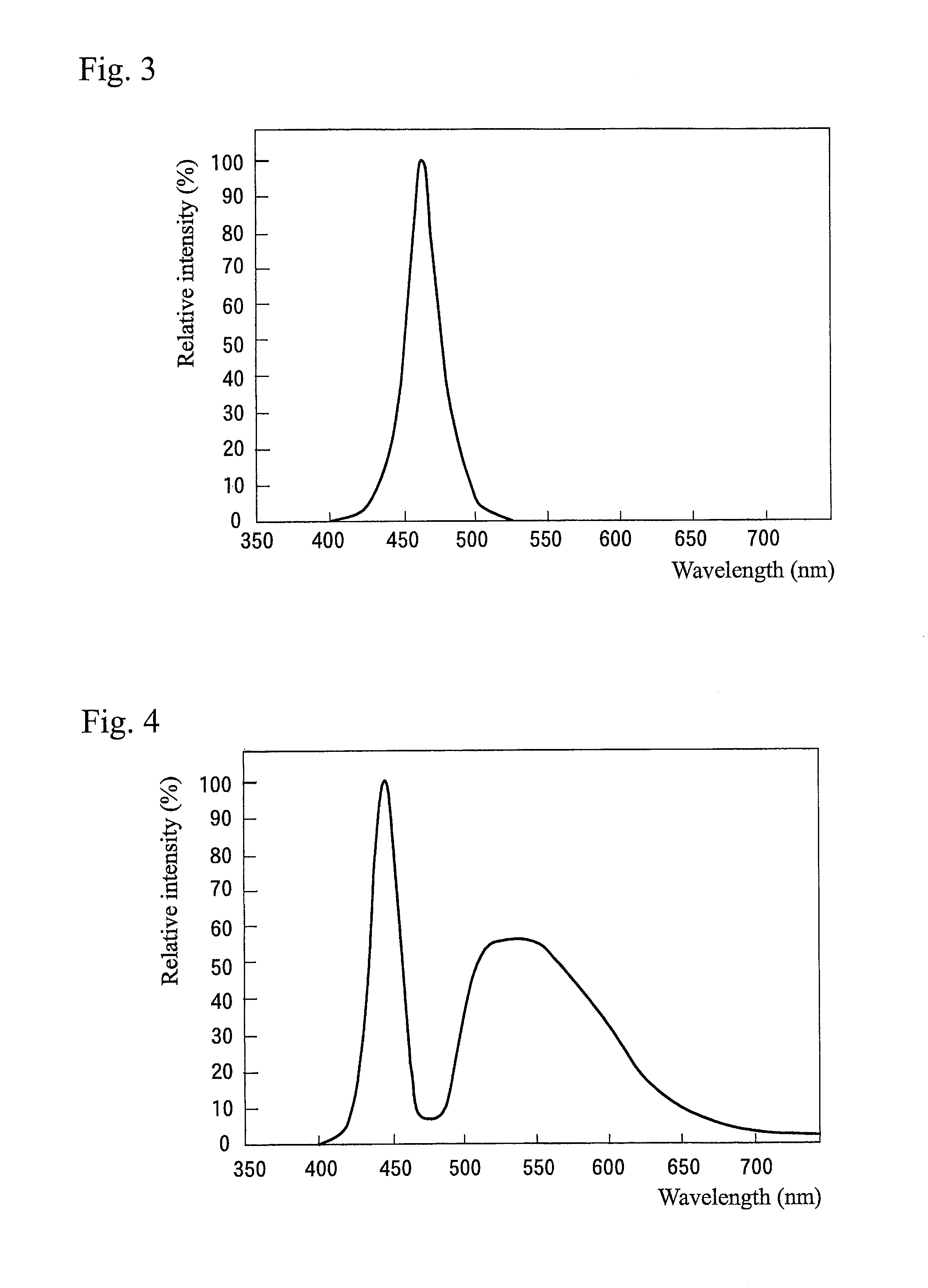
[0108]Samples used in measurement are described.
[0109]First, a thin nickel film is formed on each acrylic resin particle by electrolytic plating as the base layer. Next, sputtering is performed on three different sputtering targets, each containing Ag, Bi, and Nd with the content ratio of Bi set to at least 0.1 weight and at most 3.0 weight and the content ratio of Nd set to at least 0.1 weight % and at most 2.0 weight % with respect to the total weight of Ag, Bi, and Nd of 100 weight %. The light reflecting layer is formed through the sputtering on a surface of the base layer in each sputtering target, thereby producing three types of conductive particles.
[0110]The produced conductive particles of each type are dispersed in the binder resin to obtain an anisotropic conductive adhesive for each of Examples 1 to 3. The thin nickel film has a thickness of 0.10 μm, and the light reflecting layer has a thickness of 0.2 μm.
[0111]The compositions of the sputtering targets used to form the...
PUM
| Property | Measurement | Unit |
|---|---|---|
| reflectance | aaaaa | aaaaa |
| wavelength | aaaaa | aaaaa |
| wavelength | aaaaa | aaaaa |
Abstract
Description
Claims
Application Information
 - R&D
- Intellectual Property
- Life Sciences
- Materials
- Tech Scout
- Unparalleled Data Quality
- Higher Quality Content
- 60% Fewer Hallucinations
Browse by: Latest US Patents, China's latest patents, Technical Efficacy Thesaurus, Application Domain, Technology Topic, Popular Technical Reports.
© 2025 PatSnap. All rights reserved.Legal|Privacy policy|Modern Slavery Act Transparency Statement|Sitemap|About US| Contact US: help@patsnap.com