
Touch sensor applied on large size display

a technology of touch sensor and large display, applied in the field of touch sensor, can solve the problems of inability to apply ics to a large display, limit the number of pins of ics used, etc., and achieve the effect of low cos

Active Publication Date: 2016-12-06
E INK HLDG INC
View PDF21 Cites 0 Cited by
  • Summary
  • Abstract
  • Description
  • Claims
  • Application Information

AI Technical Summary

Benefits of technology

[0009]A touch sensor with low cost and capable of being applied on a large size display is provided. In accordance with one embodiment of the present invention, a touch sensor includes a substrate, a touch sensing layer, a first processor, and a second processor. The substrate includes a first area and a second area on the same surface of the substrate. The touch sensing layer is disposed on the substrate, and it includes a first group of conductive patterns and a second group of conductive patterns. The first group of conductive patterns is disposed on the first area of the substrate, and includes a plurality of first conductive patterns. The second group of conductive patterns is disposed on the second area of the substrate, and includes a plurality of second conductive patterns. The first processor is electrically connected to the first conductive patterns. The second processor is electrically connected to the second conductive patterns.

Problems solved by technology

However, since there is a limit in the number of pins for the ICs used in the SITO, the ICs cannot be applied to a large size display.

Method used


Image

  • Touch sensor applied on large size display
  • Touch sensor applied on large size display
  • Touch sensor applied on large size display

Examples


Embodiment Construction

[0021]Reference will now be made in detail to the present embodiments of the invention, examples of which are illustrated in the accompanying drawings. Wherever possible, the same reference numbers are used in the drawings and the description to refer to the same or like parts.

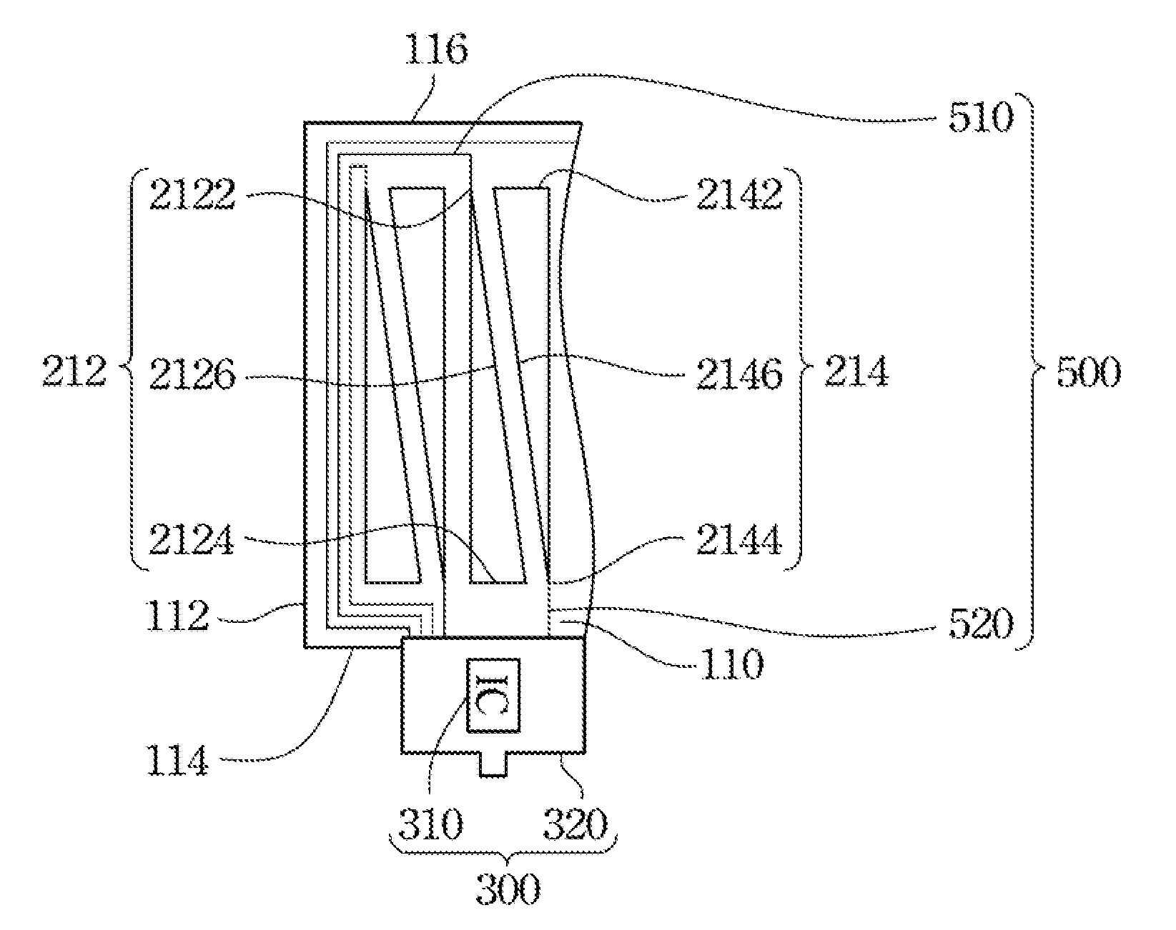
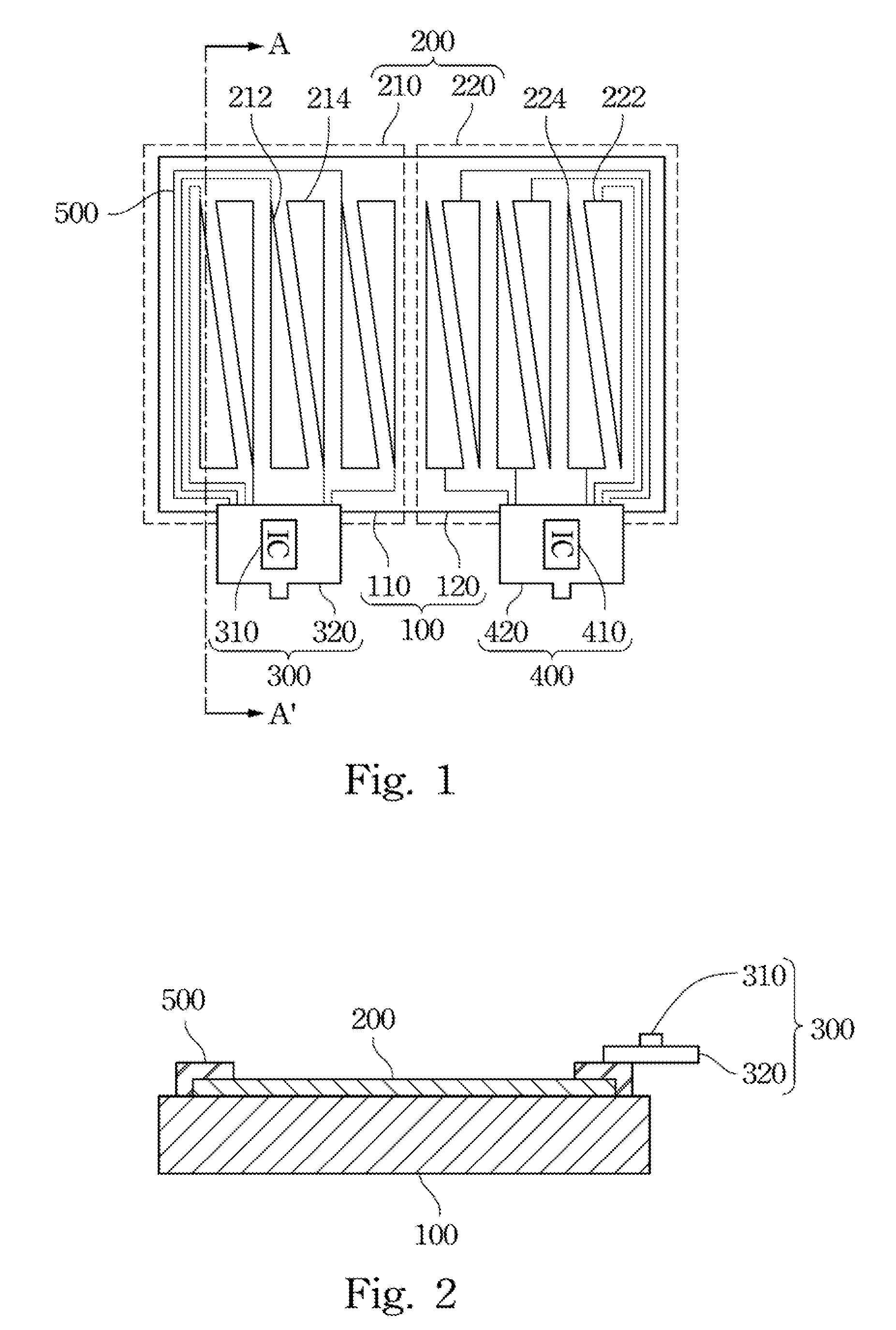
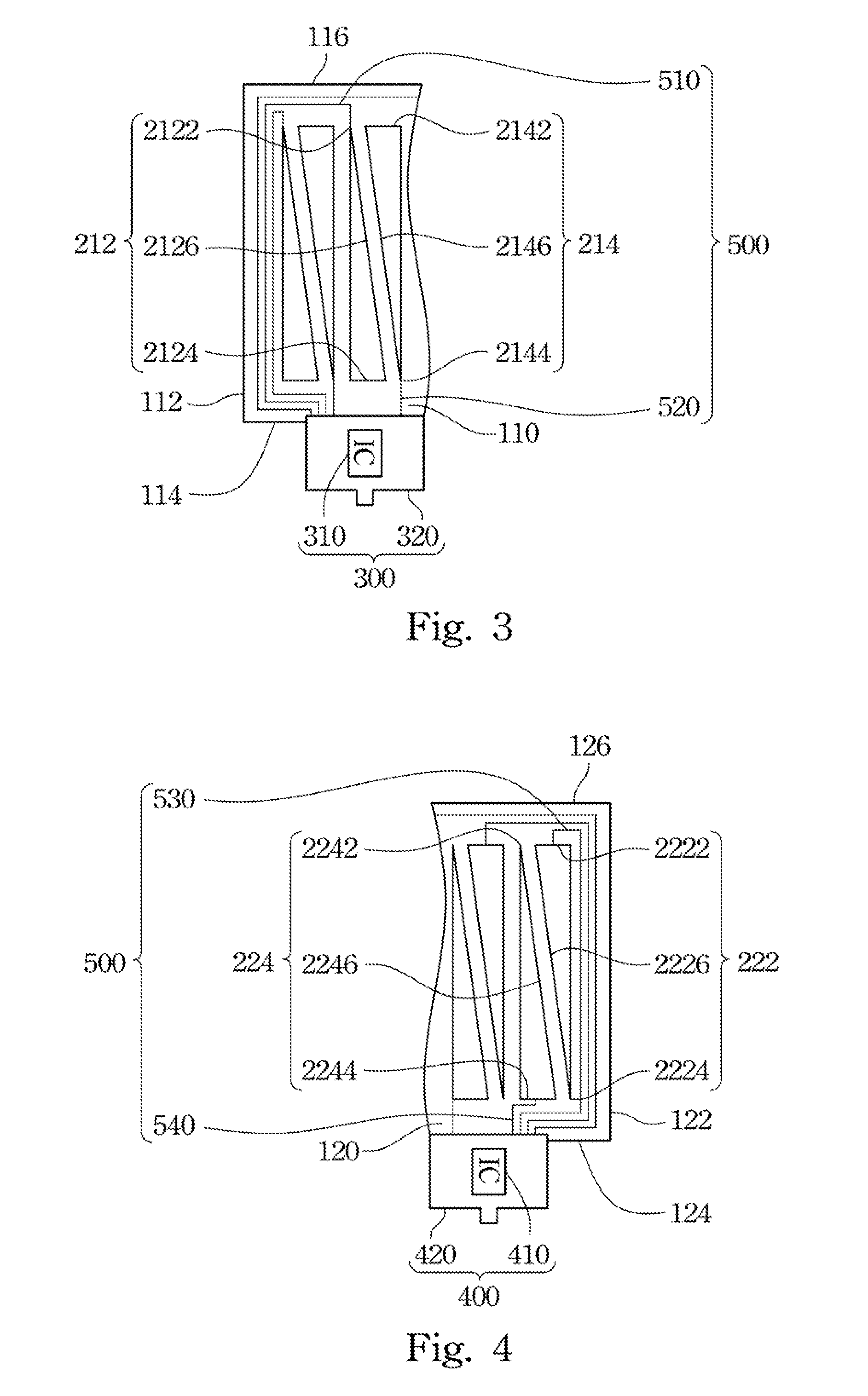
[0022]FIG. 1 is a top view of a touch sensor in accordance with one embodiment of the present invention. FIG. 2 is a cross-sectional view of the touch sensor along A-A′ ling in FIG. 1. As shown in FIG. 1 and FIG. 2, a touch sensor includes a substrate 100, a touch sensing layer 200, a first processor 300, and a second processor 400. The substrate 100 includes a first area 110 and a second area 120 on the same surface of the substrate 100. The touch sensing layer 200 is disposed on the substrate 100, and it includes a first group of conductive patterns 210 and a second group of conductive patterns 220. The first group of conductive patterns 210 is disposed on the first area 110 of the substrate 100, and include...


PUM


Abstract

A touch sensor includes a substrate, a touch sensing layer, a first processor and a second processor. The substrate includes a first area and a second area. The first area and the second area are on the same surface of the substrate. The touch sensing layer is disposed on the substrate, and includes a first group of conductive patterns and a second group of conductive patterns. The first group of conductive patterns is disposed on the first area, and includes a plurality of first conductive patterns. The second group of conductive patterns is disposed on the second area, and includes a plurality of second conductive patterns. The first processor is electrically connected to the first conductive patterns. The second processor is electrically connected to the second conductive patterns.

Description

RELATED APPLICATIONS[0001]This application claims priority to Taiwanese Application Serial Number 10117489, filed Oct. 11, 2012, which is herein incorporated by reference.BACKGROUND[0002]1. Technical Field[0003]Embodiments of the present invention relate to a sensor device. More particularly, embodiments of the present invention relate to a touch sensor.[0004]2. Description of Related Art[0005]With the development of technology, the touch panel has been widely applied in the display, such as the display of a tablet or a smart phone. By integrating the touch panel into the display, a user can directly enter commands by using a finger or a touch pen to touch the touch panel, and this operation method is more convenient than the operational method by using a traditional keypad.[0006]Generally, the touch panel is classified as a resistive touch panel, a capacitive touch panel, an optical touch panel, a sound wave touch panel, and so on. The capacitive touch panel utilizes the current in...

Claims


Application Information

Patent Timeline
Patent Type & Authority Patents(United States)
IPC IPC(8): G06F3/041G06F3/044
CPCG06F3/041G06F3/044G06F3/0416G06F3/04164G06F3/0443
Inventor HSIEH, YUN-NANCHEN, LIN-AN
Owner E INK HLDG INC
Learn More