Wafer level packaging for proximity sensor
a proximity sensor and wafer level technology, applied in wave based measurement systems, instruments, reradiation, etc., can solve the problems of high defect rate and increase manufacturing costs, and achieve the effect of reducing defect rates
- Summary
- Abstract
- Description
- Claims
- Application Information
AI Technical Summary
Benefits of technology
Problems solved by technology
Method used
Image

Examples
Embodiment Construction
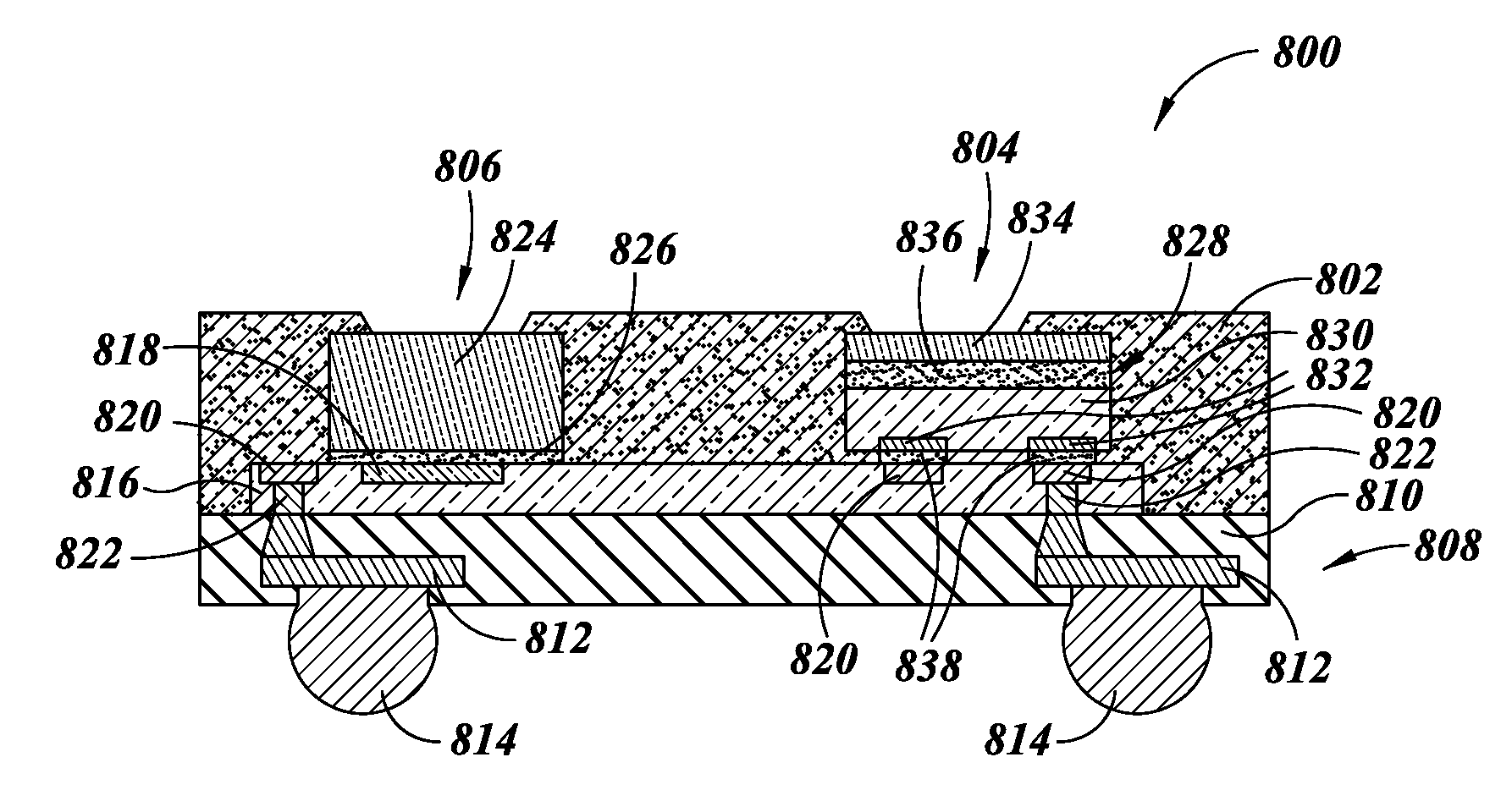
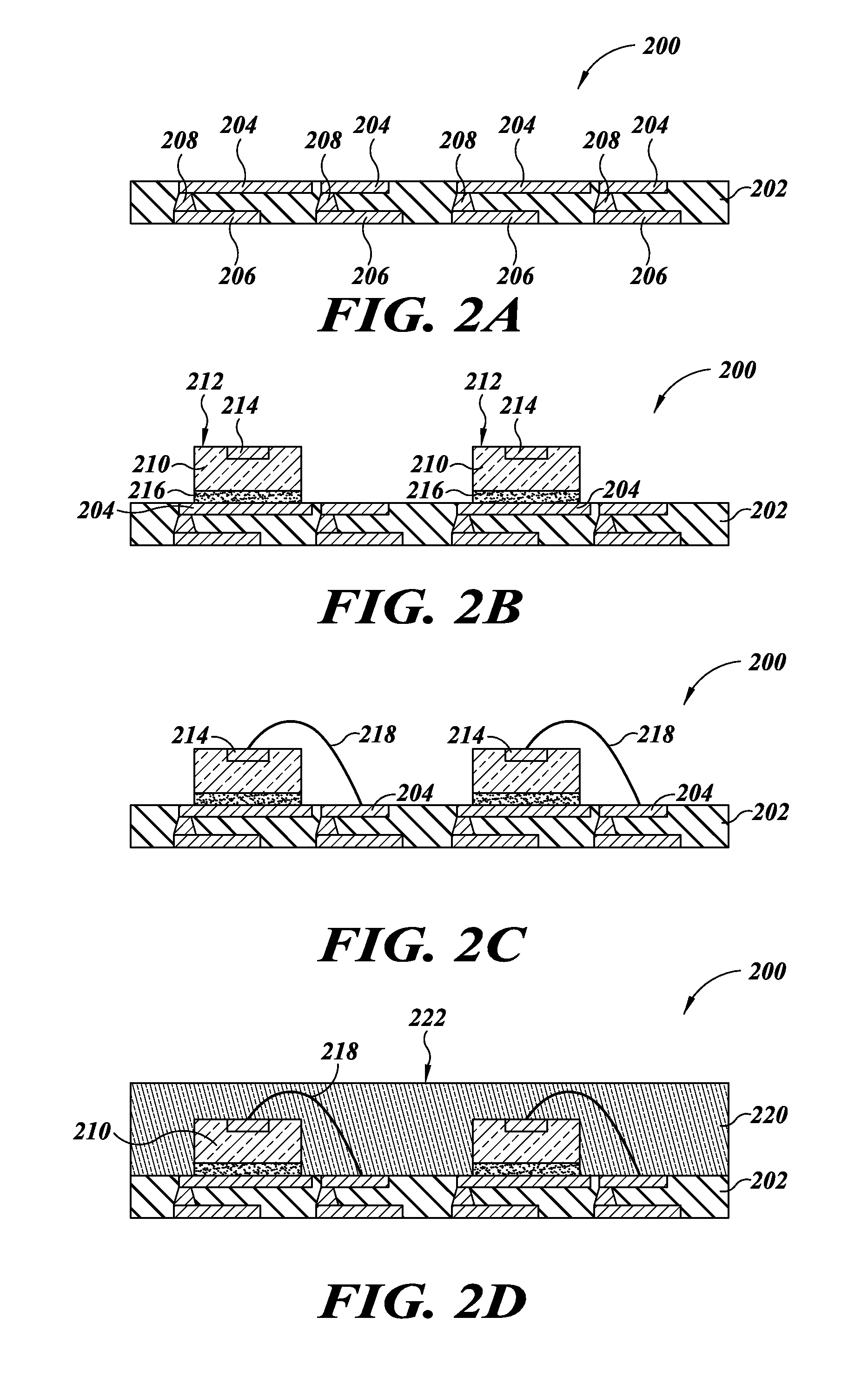
[0023]FIGS. 2A-2E show a semiconductor assembly 200 at various stages of fabrication, according to one embodiment. As shown in FIG. 2A, the semiconductor assembly 200 includes a printed circuit board substrate 202. An upper surface of the printed circuit board substrate 202 includes a plurality of contact pads 204. A lower surface of the printed circuit board substrate 202 includes a plurality of contact pads 206. A plurality conductive traces 208 form electrical connections between one or more of the contact pads 204 on the upper surface of the printed circuit board substrate 202 and one or more of the contact pads 206 on the lower surface of the printed circuit board substrate 202.
[0024]As shown in FIG. 2B, a plurality of conventional light emitting devices 210 is placed over the upper surface of the printed circuit board substrate 202. In one embodiment, each of the light emitting devices 210 is a conventional light emitting diode (LED). In one embodiment, each of the light emitt...
PUM
 Abstract
Description
Claims
Application Information
 - R&D
- Intellectual Property
- Life Sciences
- Materials
- Tech Scout
- Unparalleled Data Quality
- Higher Quality Content
- 60% Fewer Hallucinations
Browse by: Latest US Patents, China's latest patents, Technical Efficacy Thesaurus, Application Domain, Technology Topic, Popular Technical Reports.
© 2025 PatSnap. All rights reserved.Legal|Privacy policy|Modern Slavery Act Transparency Statement|Sitemap|About US| Contact US: help@patsnap.com