Liquid crystal display

a liquid crystal display and display technology, applied in the field of liquid crystal display, can solve the problems of reducing image quality, reducing transmittance, and preventing change of gray levels, so as to reduce (and prevent) deterioration.

Active Publication Date: 2017-04-04
SAMSUNG DISPLAY CO LTD
View PDF17 Cites 0 Cited by
  • Summary
  • Abstract
  • Description
  • Claims
  • Application Information

AI Technical Summary

Benefits of technology

[0013]An aspect of an embodiment of the present invention is directed toward a liquid crystal display for clarifying a change of transmittance caused by a change of gray levels and reducing (e.g., preventing) deterioration of (e.g., reduction of) transmittance while having lateral visibility approaching (or matching) front visibility.
[0026]The liquid crystal display, according to the example embodiment of the present invention, utilizes the first sub-pixel electrode to which the first voltage is applied and the second sub-pixel electrode to which the second voltage is applied, divides one pixel area into four regions respectively having a different electric field intensity, causes the lateral visibility to approach the front visibility, clarifies the change of transmittance induced by the change of gray levels, and reduces (e.g., prevents) deterioration of (e.g., reduction of) transmittance that may occur in the region between the first sub-pixel electrode and the second sub-pixel electrode.

Problems solved by technology

However, when the side visibility is close to the front visibility by dividing one pixel into two subpixels and making the transmittance different, luminance is increased at a low gray level or a high gray level, such that it is difficult to represent a gray level at the side, thereby causing the reduction in image quality.
Further, when a change of transmittance is unclear according to a change of gray levels, the change of gray levels is not expressed and displaying quality may be deteriorated (e.g., reduced).

Method used


Image

  • Liquid crystal display
  • Liquid crystal display
  • Liquid crystal display

Examples


Embodiment Construction

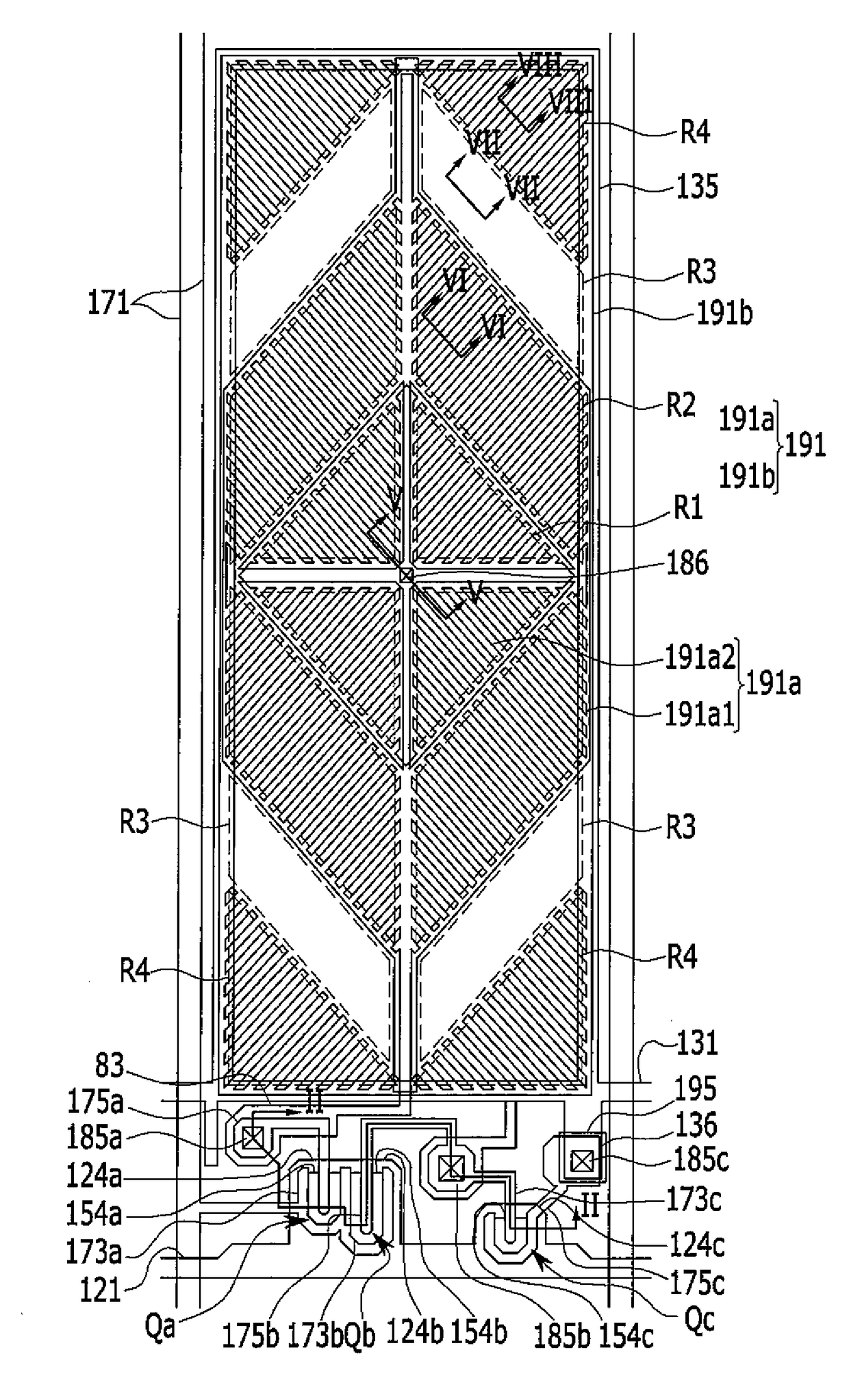
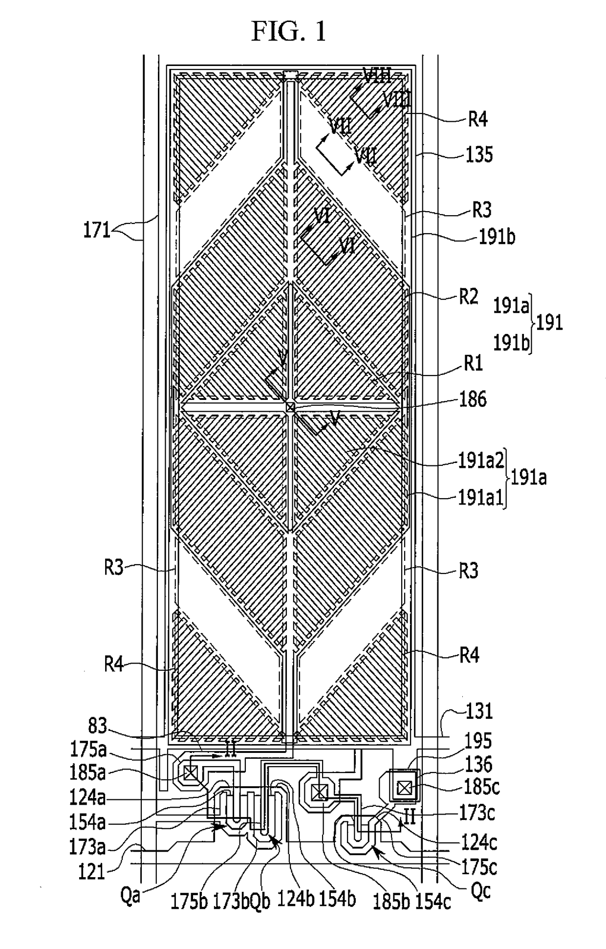
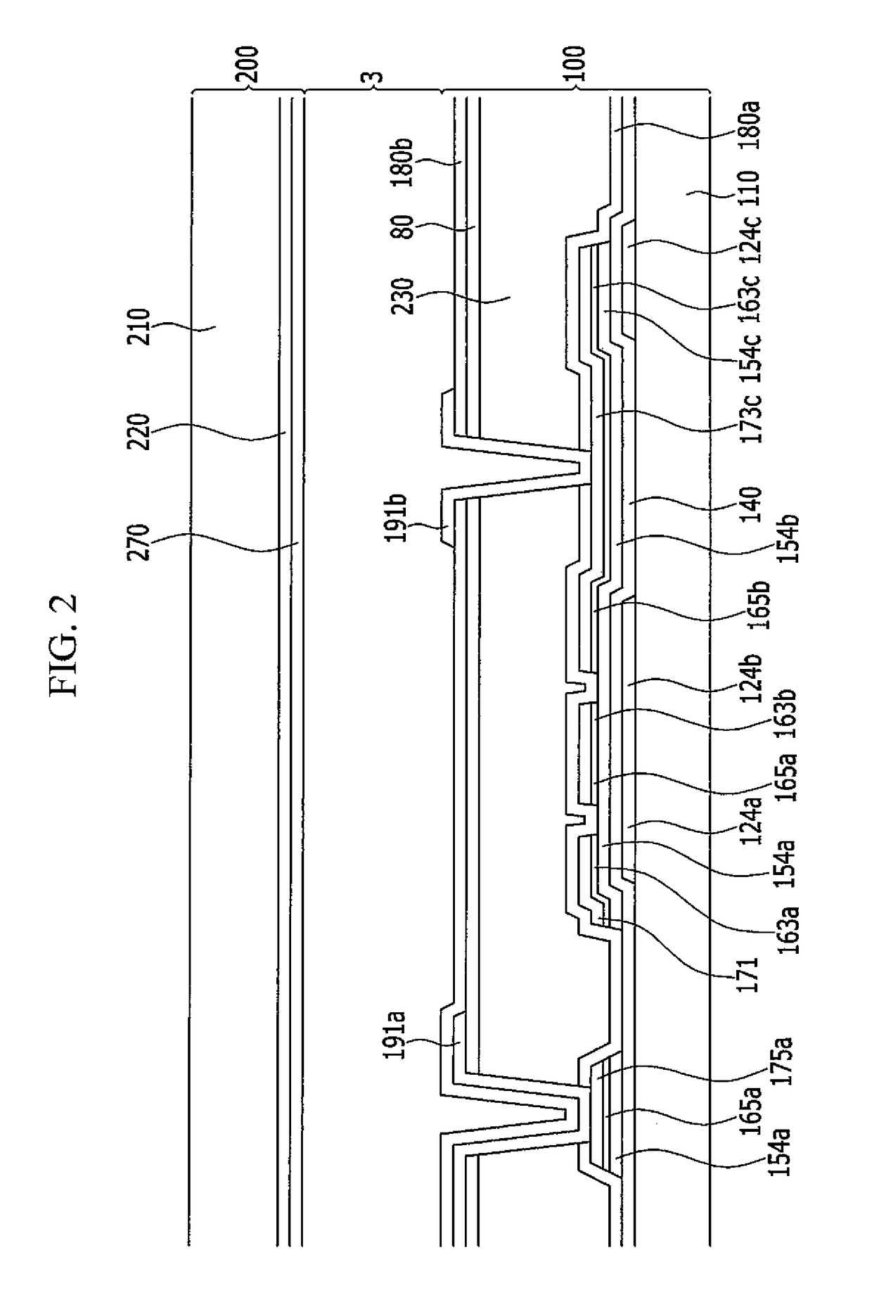
[0069]Example embodiments of the present invention will be described in more detail with reference to the attached drawings. The present invention may be modified in many different forms, and should not be construed as being limited to the example embodiments set forth herein. Rather, the example embodiments of the present invention are provided so that this disclosure will be thorough and complete, and will fully convey the concept of the present invention to those skilled in the art.

[0070]In the drawings, the thickness of layers and regions may be exaggerated for clarity. In addition, when a layer is described to be formed on another layer or on a substrate, this means that the layer may be formed on the other layer or on the substrate, or a third layer may be interposed between the layer and the other layer or the substrate. Like numbers refer to like elements throughout the specification.

[0071]It will be understood that, although the terms “first”, “second”, “third”, etc., may b...


PUM


Abstract

A liquid crystal display including a first substrate, a first sub-pixel electrode on the first substrate and configured to receive a first voltage, a second sub-pixel electrode on the first substrate and configured to receive a second voltage, an insulating layer between the first sub-pixel electrode and the second sub-pixel electrode, a second substrate facing the first substrate, and a common electrode on the second substrate, wherein the first sub-pixel electrode includes a first sub-region below the insulating layer and a second sub-region above the insulating layer, wherein the second sub-region of the first sub-pixel electrode includes a plurality of first branch electrodes, wherein the second sub-pixel electrode is above the insulating layer, and wherein a difference between the first voltage and a common voltage is greater than a difference between the second voltage and the common voltage.

Description

CROSS-REFERENCE TO RELATED APPLICATION[0001]This application claims priority to and the benefit of Korean Patent Application No. 10-2014-0076073, filed in the Korean Intellectual Property Office on Jun. 20, 2014, the entire content of which is incorporated herein by reference.BACKGROUND[0002]1. Field[0003]An aspect of the present invention relates to a liquid crystal display.[0004]2. Description of the Related Art[0005]A liquid crystal display, which is one of the flat panel displays most widely used at present, includes two display panels on which electric field generating electrodes such as a pixel electrode and a common electrode are formed, and has a liquid crystal layer inserted therebetween.[0006]The liquid crystal display displays an image by generating an electric field on a liquid crystal layer by applying a voltage to the electric field generating electrodes, determining alignments of liquid crystal molecules of the liquid crystal layer through the generated electric field...

Claims


Application Information

Patent Timeline
Patent Type & Authority Patents(United States)
IPC IPC(8): G09G3/28G09G3/36
CPCG09G3/3659G09G3/3648G09G2300/0426G09G2300/0447G02F1/134309G02F2201/123G02F1/134372
Inventor JUNG, JAE HOONKIM, HYO SIKSHIN, KI CHULYANG, DAN BIHONG, JI PHYO
Owner SAMSUNG DISPLAY CO LTD
Why Eureka
Try Eureka