Array substrate, manufacturing method of array substrate, and display device

An array substrate and pixel electrode technology, which is applied in the fields of semiconductor/solid-state device manufacturing, optics, instruments, etc., can solve the problems of reducing the display effect of the display device, affecting the shading effect of the drain, etc., so as to improve the display effect, reduce the reflection effect, The effect of reducing transmittance

Inactive Publication Date: 2014-08-13
BOE TECH GRP CO LTD
View PDF4 Cites 39 Cited by
  • Summary
  • Abstract
  • Description
  • Claims
  • Application Information

AI Technical Summary

Problems solved by technology

[0004] The inventors found that after the black matrix is ​​integrated on the array substrate, since the black matrix is ​​usually located between the drain and the pixel electrode of the thin film transistor, in order to realize the electrical connection between the drain and the pixel electrode, it needs to be formed after the black matrix is ​​formed. The via hole will affect the light-shielding effect of the black matrix on the drain, causing the drain to reflect light from the side of the via hole, reducing the display effect of the display device

Method used


Image

  • Array substrate, manufacturing method of array substrate, and display device
  • Array substrate, manufacturing method of array substrate, and display device
  • Array substrate, manufacturing method of array substrate, and display device

Examples


Embodiment 1

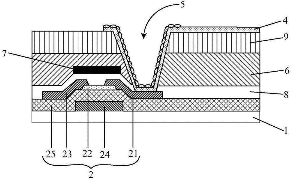
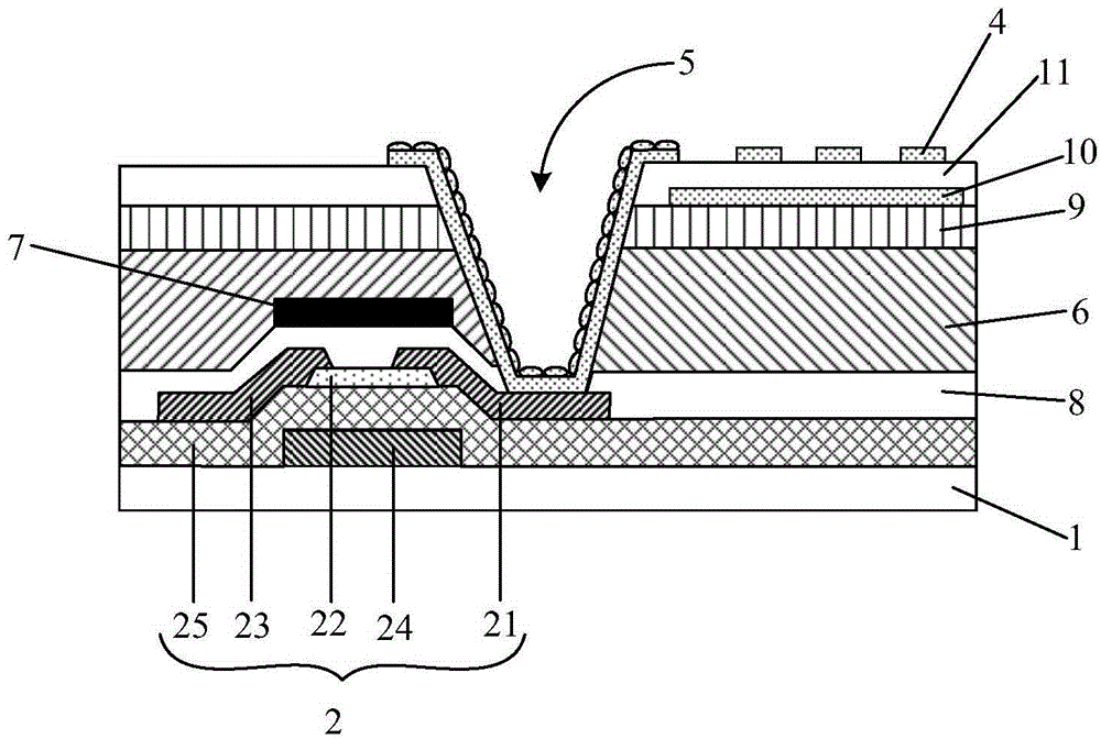
[0037] An embodiment of the present invention provides an array substrate, such as figure 1 As shown, the array substrate includes:

[0038] The drain 21, the insulating layer 3 and the pixel electrode 4 of the thin film transistor unit 2 located on the base substrate 1, the insulating layer 3 is located between the drain 21 and the pixel electrode 4, the insulating layer 3 A via hole 5 is formed through which the drain electrode 21 and the pixel electrode 4 are connected; wherein, the surface of the pixel electrode 4 at the via hole 5 is a rough surface.

[0039] In the embodiment of the present invention, the COA technology is adopted, and the color filter 6 , the black matrix 7 and the TFT unit 2 are all formed on the same base substrate 1 . Since the thin film transistor unit 2 mainly forms a conductive channel in the active layer 22 , the transmission of electric signals can be realized between the source 23 and the drain 21 . The light will affect the ability of the co...

Embodiment 2

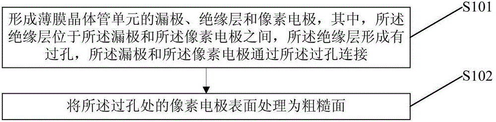
[0053] An embodiment of the present invention provides a method for preparing an array substrate, such as image 3 As shown, the preparation method of the array substrate includes:

[0054] Step S101, forming a drain, an insulating layer, and a pixel electrode of a TFT unit, wherein the insulating layer is located between the drain and the pixel electrode, the insulating layer is formed with a via hole, and the drain and The pixel electrodes are connected through the via holes;

[0055] Step S102 , processing the surface of the pixel electrode at the via hole to a rough surface.

[0056] Wherein, step S102 includes: treating the pixel electrode at the via hole with plasma, so that the surface of the pixel electrode at the via hole is a rough surface.

[0057] Specifically, when processing the surface of the pixel electrode 4 at the via hole 5, it is necessary to use a photoresist to form a protective layer to protect the pixel electrode that does not need to be processed, an...


PUM


Abstract

The embodiment of the invention discloses an array substrate, a manufacturing method of the array substrate, and a display device, and relates to the technical field of displaying. A drain electrode can be prevented from reflecting light, and the display effect of the display device is guaranteed. The array substrate comprises the drain electrode, an insulating layer and a pixel electrode of a thin film transistor unit, wherein the insulating layer is located between the drain electrode and the pixel electrode and provided with a via hole, the drain electrode and the pixel electrode are connected through the via hole, and the surface, at the via hole, of the pixel electrode is rough.

Description

technical field [0001] The present invention relates to the field of display technology, in particular to an array substrate, a preparation method thereof, and a display device. Background technique [0002] In recent years, people have higher and higher requirements on light transmittance, resolution, and power consumption of display devices, and display devices are developing towards high transmittance, high resolution, and low power consumption. Among them, the higher the resolution, the smaller the size of each pixel unit. When the side length of the pixel unit changes from tens of microns to more than ten microns, obviously, the size of the pixel unit has been greatly reduced. At this time , if the width of the black matrix dividing the pixel units remains unchanged, the black matrix will become obvious relative to the pixel units, which will affect the display effect of the display device. [0003] Therefore, one of the integration technologies (Color Filter on Array,...

Claims


Application Information

Patent Timeline
Patent Type & Authority Applications(China)
IPC IPC(8): H01L27/12H01L23/528H01L21/77
CPCG02F1/134363G02F1/136209G02F1/136227G02F1/136222H01L27/124H01L2924/0002H01L2924/00H01L27/1262
Inventor 张锋曹占锋姚琪舒适
Owner BOE TECH GRP CO LTD
Why Eureka
Try Eureka