
Address detection circuit, memory system including the same

a detection circuit and address technology, applied in the field of integrated circuit design technology, can solve problems such as data likely to be degraded, and achieve the effect of preventing data from being degraded

Active Publication Date: 2017-05-09
SK HYNIX INC
View PDF11 Cites 0 Cited by
  • Summary
  • Abstract
  • Description
  • Claims
  • Application Information

AI Technical Summary

Benefits of technology

[0014]Further, other embodiments of the present invention are directed to a memory system that may prevent data from being degraded due to word line disturbance, by using address detection.
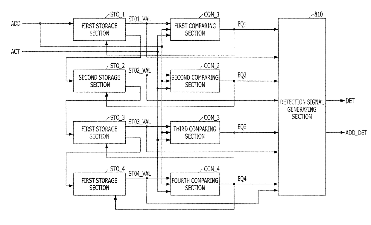
[0046]In accordance with the above embodiments, by storing recently inputted addresses and comparing the stored addresses with a currently inputted address, it may possible to detect an address with a high input frequency.
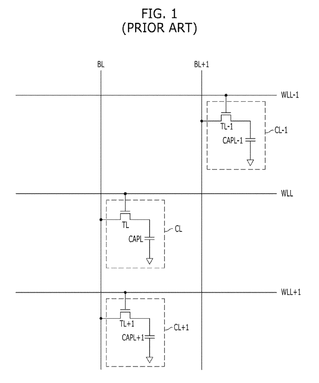
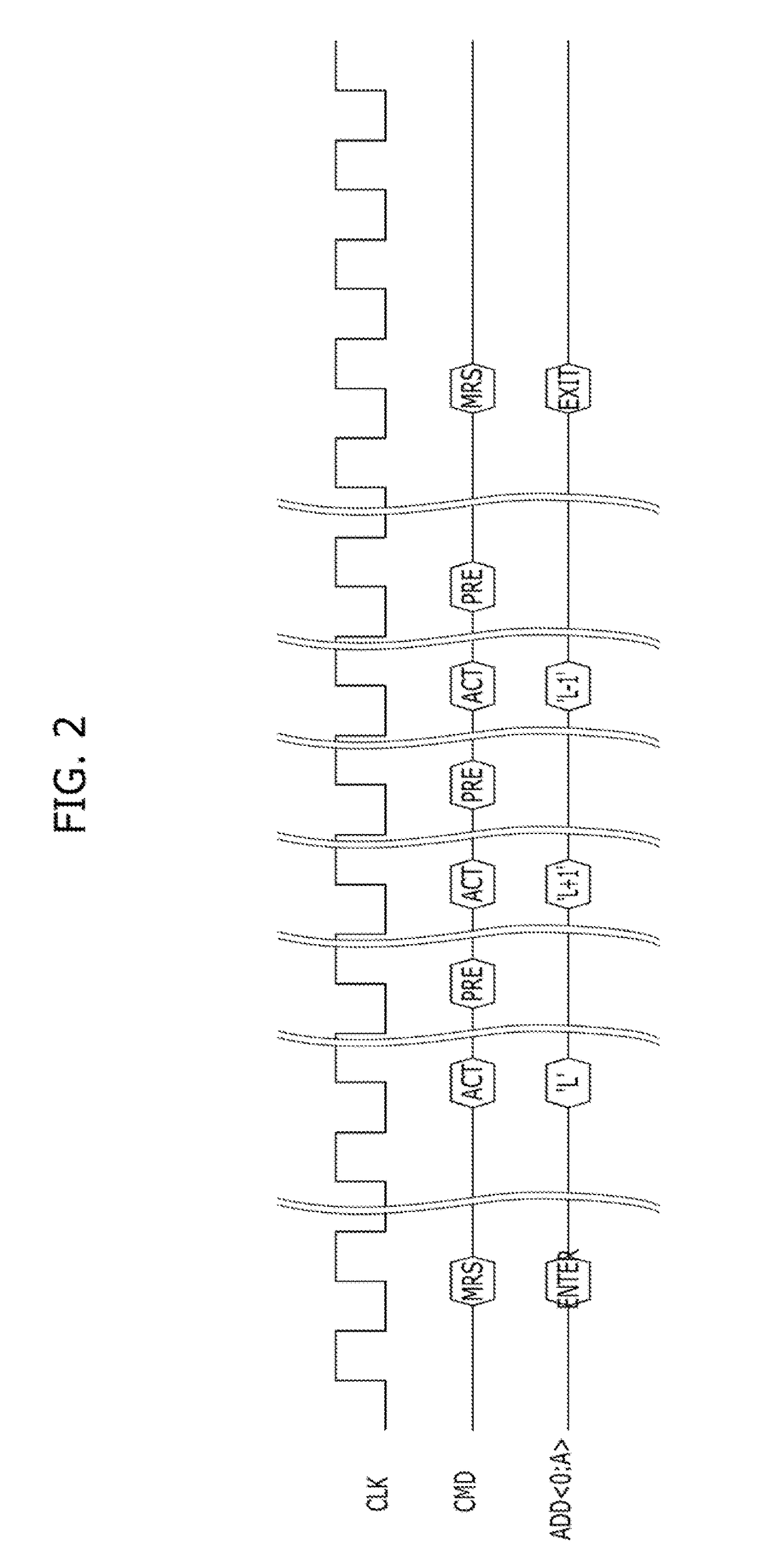
[0048]Further described in the embodiments is that by refreshing adjacent word lines of a word liner with a high activation frequency (i.e., a frequently activated word line), by using a detected address, it may be possible to prevent data from being degraded due to word line disturbance.

Problems solved by technology

Furthermore, as electromagnetic waves, which are generated while the word line toggles between the activated state and the deactivated state, introduce or discharge electrons into or from the cell capacitors of the memory cells connected with adjacent word lines, data are likely to be degraded.

Method used


Image

  • Address detection circuit, memory system including the same
  • Address detection circuit, memory system including the same
  • Address detection circuit, memory system including the same

Examples


Embodiment Construction

[0060]Various embodiments will be described below in more detail with reference to the accompanying drawings. The present invention may, however, be embodied in different forms and should not be construed as limited to the embodiments set forth herein. Rather, these embodiments are provided so that this disclosure will be thorough and complete, and will fully convey the scope of the present invention to those skilled in the art. Throughout the disclosure, reference numerals correspond directly to the like numbered parts in the various figures and embodiments of the present invention. It is also noted that in this specification, “connected coupled” refers to one component not only directly coupling another component but also indirectly coupling another component through an intermediate component. In addition, a singular form may include a plural form as long as it is not specifically mentioned in a sentence.

[0061]In the following descriptions, a high input frequency address means an ...


PUM


Abstract

An address detection circuit includes an address storage unit suitable for receiving an address when an active command is activated, and storing recently inputted N number of addresses; and an address determination unit suitable for determining whether an address currently inputted to the address storage unit is already inputted at least a threshold number of times in each period that the active command is activated M (1≦M≦N) number of times, based on the N number of addresses stored in the address storage unit.

Description

CROSS-REFERENCE TO RELATED APPLICATIONS[0001]The present application claims priority of Korean Patent. Application No. 10-2013-0060475, filed on May 28, 2013, which is incorporated herein by reference in its entirety.BACKGROUND[0002]1. Field[0003]Exemplary embodiments of the present invention relate to an integrated circuit design technology, and more particularly, to an address detection circuit, a memory system, and an address detection method.[0004]2. Description of the Related Art[0005]As the degree of integration of a memory increases, a space between word lines included in the memory such as a DRAM is reduced. As the space between the word lines is reduced a coupling effect between adjacent word lines may increase.[0006]When data is inputted or outputted to or from a memory cell, a word line toggles between an activated state and a deactivated state. In this regard, the coupling effect between adjacent word lines may increase and the data of a memory cell connected with a word...

Claims


Application Information

Patent Timeline
Patent Type & Authority Patents(United States)
IPC IPC(8): G11C8/00G11C11/408G11C11/406
CPCG11C11/408G11C11/406G11C11/401G11C11/4063
Inventor KIM, CHANG-HYUNSONG, CHOUNG-KI
Owner SK HYNIX INC
Learn More