Method for driving liquid crystal display device

a liquid crystal display device and display device technology, applied in semiconductor devices, instruments, computing, etc., can solve the problems of display deterioration, reduced detection accuracy in image capture, and difficult to improve the characteristics of elements, so as to achieve sufficient imaging period, improve image quality and detection accuracy in image capture, and increase the frequency of image signal input to each pixel of the liquid crystal display device.

Inactive Publication Date: 2016-05-19
SEMICON ENERGY LAB CO LTD
View PDF0 Cites 0 Cited by
  • Summary
  • Abstract
  • Description
  • Claims
  • Application Information

AI Technical Summary

Benefits of technology

The present invention relates to improving image quality and detection accuracy in image capture of liquid crystal display devices. The invention achieves this by increasing the frequency of input of image signals and securing a sufficient imaging period. This reduces the frequency of input of image signals and suppresses display deterioration, such as color break, which improves image quality and detection accuracy. The invention allows image signals to be concurrently supplied to pixels provided in a plurality of rows among pixels arranged in matrix, and image capture can be concurrently performed in pixels provided in a plurality of rows among pixels arranged in matrix.

Problems solved by technology

However, it is not easy to improve the characteristics of the elements.
Moreover, shortening an imaging period may cause a reduction in detection accuracy in image capture.
However, display deterioration such as color break becomes obvious in that case, which is a problem.

Method used


Image

  • Method for driving liquid crystal display device
  • Method for driving liquid crystal display device
  • Method for driving liquid crystal display device

Examples


embodiment 1

[0064]In this embodiment, a liquid crystal display device in one embodiment of the present invention will be described with reference to FIG. 1, FIGS. 2A to 2C, FIGS. 3A and 3B, FIGS. 4A and 4B, FIG. 5, FIG. 6, FIG. 7, FIGS. 8A and 8B, FIGS. 9A and 9B, FIGS. 10A and 10B, and FIG. 11.

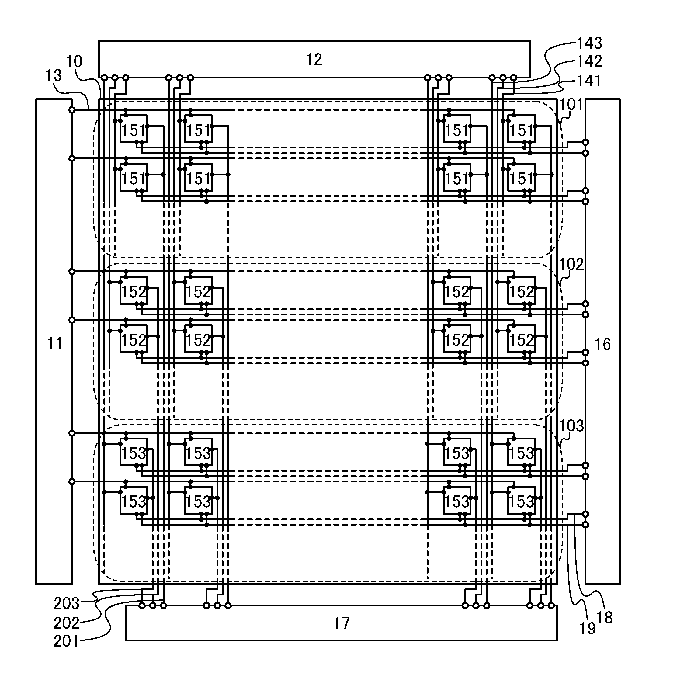
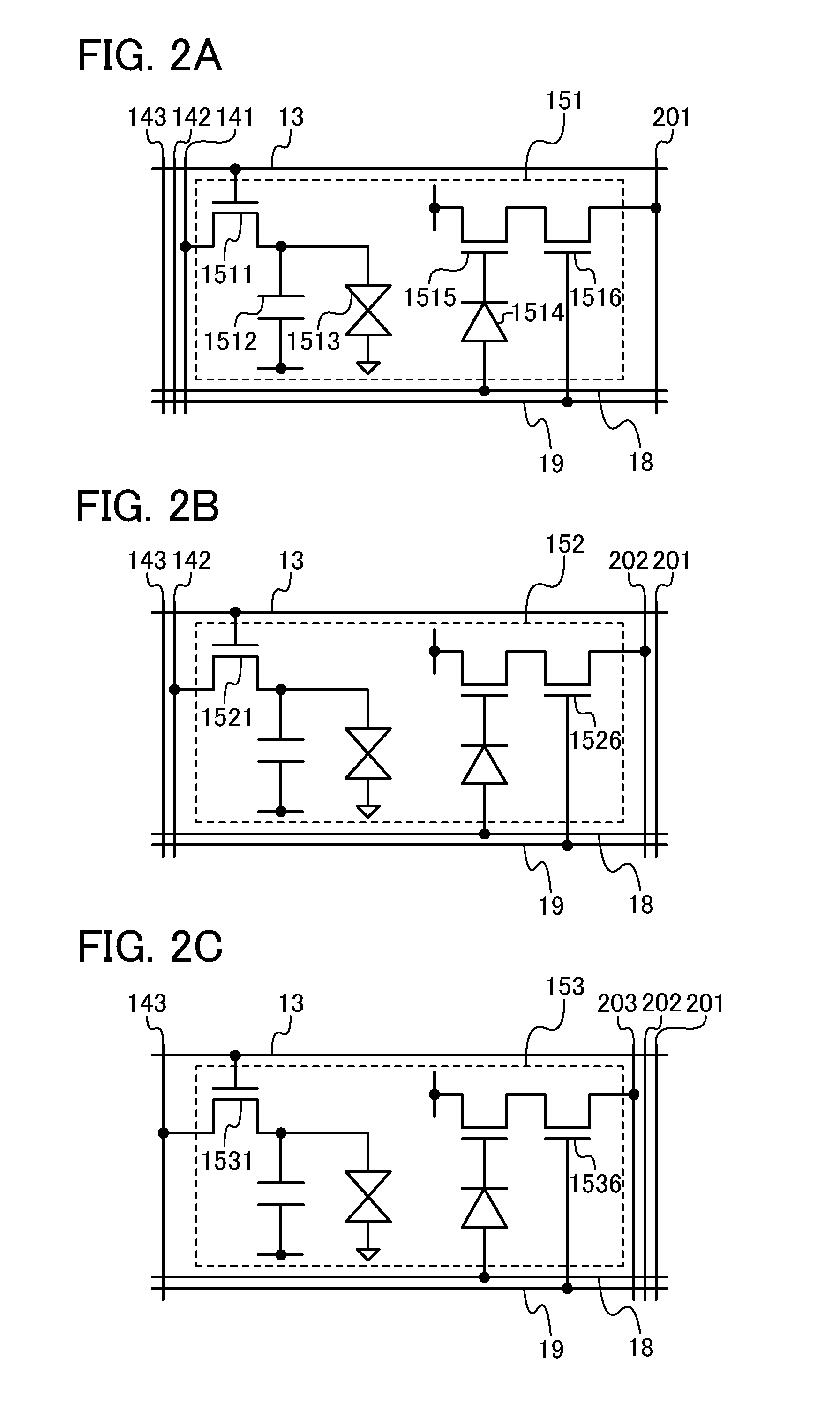
[0065]FIG. 1 illustrates a structure example of a liquid crystal display device. The liquid crystal display device illustrated in FIG. 1 includes a pixel portion 10; a scan line driver circuit 11; an image signal line driver circuit 12; an image sensor driver circuit 16; a detection circuit 17; m (m is a natural number of 3 or more) scan lines 13 which are arranged parallel or almost parallel to each other and whose potentials are controlled by the scan line driver circuit 11; n (n is a natural number of 2 or more) image signal lines 141, n image signal lines 142, and n image signal lines 143 which are arranged parallel or almost parallel to each other and whose potentials are controlled by the image sig...

embodiment 2

[0112]In this embodiment, operation of a liquid crystal display device of one embodiment of the present invention, which is different from the liquid crystal display device described in Embodiment 1 is described with reference to FIGS. 22A and 22B, FIG. 23, FIG. 24, FIG. 25, FIG. 26, FIG. 27, and FIG. 28.

[0113]As the liquid crystal display device in this embodiment, the liquid crystal display device (see FIG. 1 and FIGS. 2A to 2C) described in Embodiment 1 can be applied. Therefore, the description in Embodiment 1 is to be referred to.

[0114]As a scan line driver circuit included in the liquid crystal display device in this embodiment, the scan line driver circuit 11 (see FIG. 3A) included in the liquid crystal display device described in Embodiment 1 can be applied. Therefore, the description in Embodiment 1 is to be referred to for the structure of the scan line driver circuit.

[0115]An operation example of the scan line driver circuit 11 in this embodiment is described with referen...

embodiment 3

[0149]In this embodiment, operation of a liquid crystal display device of one embodiment of the present invention, which is different from the liquid crystal display device described in Embodiment 1 or 2 is described with reference to FIG. 29, FIG. 30, FIG. 31, FIG. 32, and FIG. 33.

[0150]As the liquid crystal display device in this embodiment, the liquid crystal display device (see FIG. 1 and FIGS. 2A to 2C) described in Embodiment 1 can be applied. Therefore, the description in Embodiment 1 is to be referred to.

[0151]As a scan line driver circuit included in the liquid crystal display device in this embodiment, the scan line driver circuit 11 (see FIG. 3A) included in the liquid crystal display device described in Embodiment 1 can be applied. Therefore, the description in Embodiment 1 is to be referred to for the structure of the scan line driver circuit. Further, the scan line driver circuit can be operated in the same manner as the scan line driver circuit described in Embodiment...


PUM


Abstract

In a field-sequential liquid crystal display device, image quality and detection accuracy in image capture are improved by increasing the frequency of input of image signals and securing a sufficient imaging period. Image signals are concurrently supplied to pixels provided in a plurality of rows among pixels arranged in matrix. Further, image capture is concurrently performed in pixels provided in a plurality of rows among pixels arranged in matrix. Thus, the frequency of input of an image signal to each pixel of the liquid crystal display device can be increased and a sufficient imaging period can be secured. As a result, in the liquid crystal display device, display deterioration such as color break which is caused in a field-sequential liquid crystal display device can be suppressed and improvements in image quality and detection accuracy in image capture can be realized.

Description

BACKGROUND OF THE INVENTION[0001]1. Field of the Invention[0002]The present invention relates to methods for driving liquid crystal display devices. In particular, the present invention relates to a field sequential liquid crystal display device capable of image capture by measure of the amount of light which is used for displaying images and reflected by an object to be read.[0003]2. Description of the Related Art[0004]As display methods of liquid crystal display devices, a color filter method and a field sequential method are known. In a color-filter liquid crystal display device, a plurality of subpixels which have color filters for transmitting only light with wavelengths of given colors (e.g., red (R), green (G), and blue (B)) are provided in each pixel. A desired color is expressed by control of transmission of white light in each subpixel and mixture of a plurality of colors in each pixel. In contrast, in a field-sequential liquid crystal display device, a plurality of light ...

Claims


Application Information

Patent Timeline
Patent Type & Authority Applications(United States)
IPC IPC(8): G09G3/36G09G3/20
CPCG09G3/3648G09G2310/08G09G3/2003G06F3/0412G06F3/042G09G3/3413G09G3/3655G09G3/3688G09G2300/0426G09G2310/0205G09G2310/0218G09G2310/0235G09G2320/0242H01L29/7869G09G3/3677
Inventor KUROKAWA, YOSHIYUKIIKEDA, TAKAYUKI
Owner SEMICON ENERGY LAB CO LTD
Why Eureka
Try Eureka