
Method for CMP of high-K metal gate structures
a metal gate and high-k technology, applied in the direction of semiconductor devices, electrical equipment, basic electric elements, etc., can solve the problems of serious affecting the performance and yield of the manufactured semiconductor device, the polysilicon gate is prone to over-polishing, and the polysilicon gate may be over-polished
- Summary
- Abstract
- Description
- Claims
- Application Information
AI Technical Summary
Benefits of technology
Problems solved by technology
Method used
Image

Examples
embodiment 1
[0039
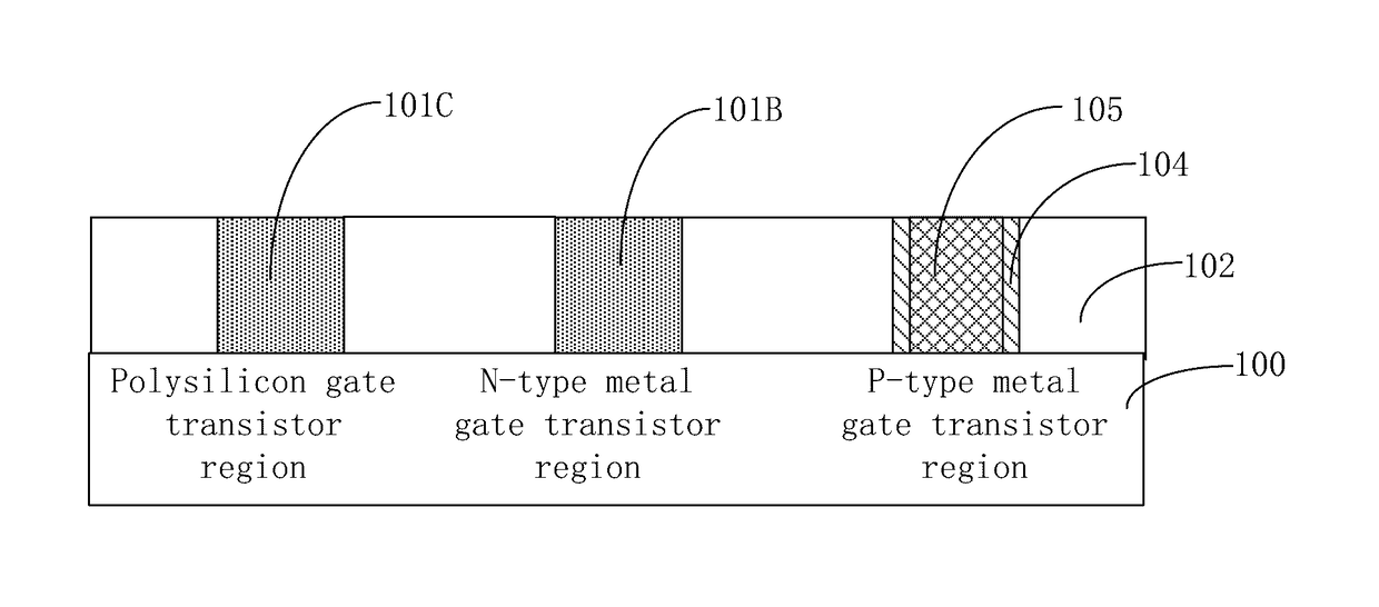
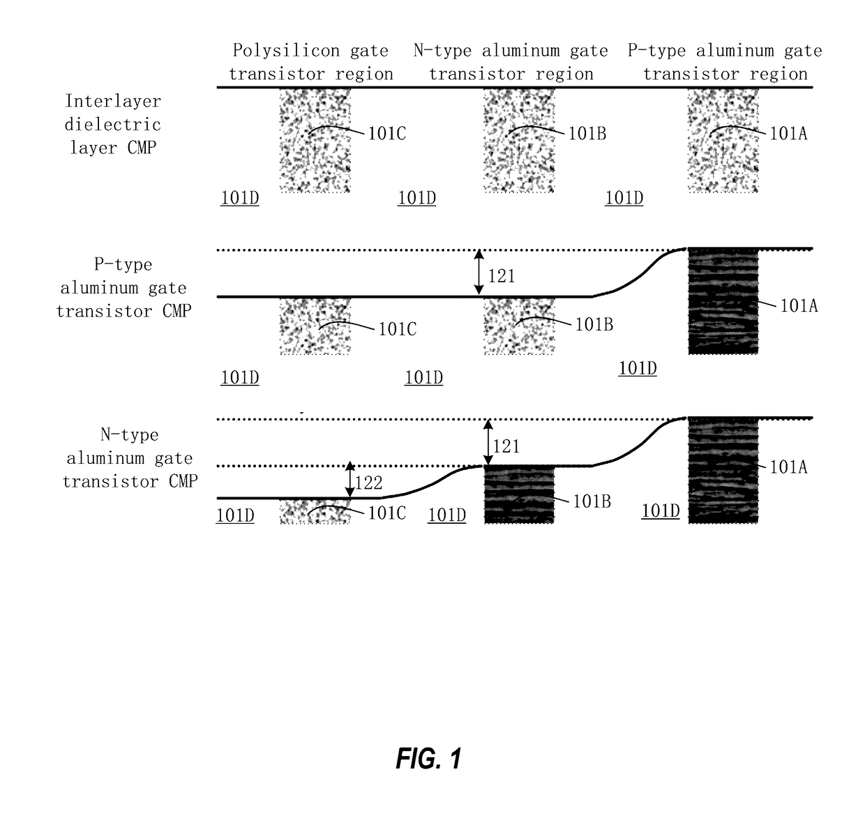
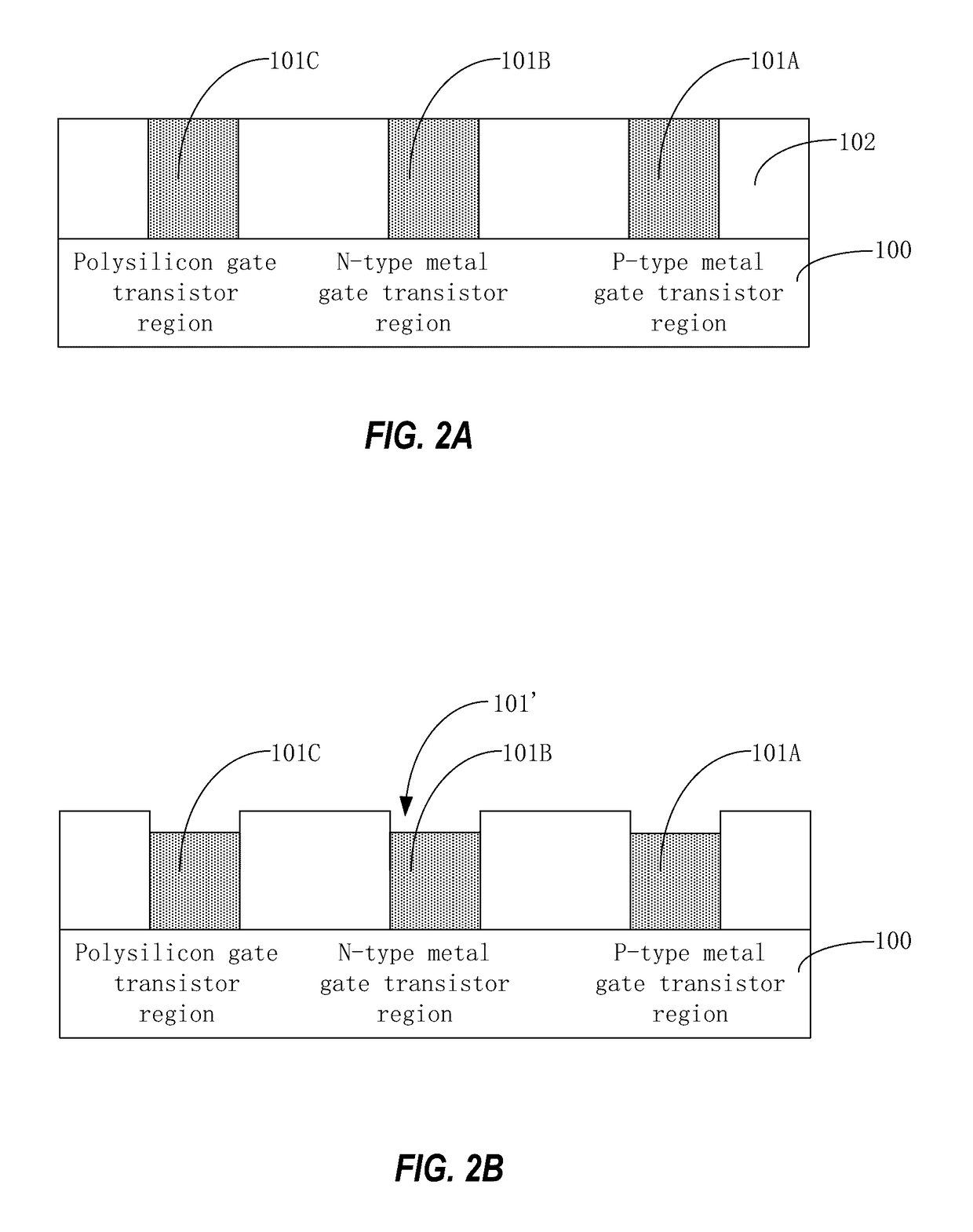
[0040]FIGS. 2A to 2F are cross-sectional views depicting stages of a method of manufacturing a semiconductor device according to an embodiment of the present invention, and FIG. 3 is a simplified flow chart of a method of manufacturing a semiconductor device according to an embodiment of the present invention. With reference to FIGS. 2A-2F and FIG. 3, a method according to the embodiment may include the following steps:
[0041]Step A1: provide a semiconductor substrate 100 comprising a front-end device, the front-end device comprising a first dummy gate 101A in a P-type metal gate transistor region, a second dummy gate 101B in an N-type metal gate transistor region, and a polysilicon gate 101C in a polysilicon gate region; and form an interlayer dielectric layer 102 on the semiconductor substrate, as shown in FIG. 2A.
[0042]In the embodiment, the front-end device is referred to as a structure that has been formed on the semiconductor substrate and may contain certain components, b...
embodiment 2
[0073
[0074]FIG. 3 is a simplified flow chart of a method 300 for manufacturing a semiconductor device according to an embodiment of the present invention. Method 300 may include:
[0075]S101: provide a semiconductor substrate comprising a front-end device, the front-end device comprising a first dummy gate in a first type metal gate transistor region, a second dummy gate in a second type metal gate transistor region, and a polysilicon gate in a polysilicon gate transistor region; form an interlayer dielectric layer on the semiconductor substrate;
[0076]S102: remove by etching a thickness of the first dummy gate, a thickness of the second dummy gate, and a thickness of the polysilicon gate so that the first dummy gate, the second dummy gate, and the polysilicon gate are below the surface of the interlayer dielectric layer;
[0077]S103: form a protective layer on the first dummy gate, the second dummy gate, and the polysilicon gate;
[0078]S104: remove by etching a portion of the protective ...
PUM
 Abstract
Description
Claims
Application Information