Printed compatible designs and layout schemes for printed electronics

a technology for printed electronics and compatible designs, applied in the direction of printed circuit non-printed electric components association, electronic components of semiconductor/solid-state devices, instruments, etc., can solve the problems of relatively large overlay allowance, poor layer to layer registration, and certain manufacturing issues of printed electronic circuits

Active Publication Date: 2013-02-26
ENSURGE MICROPOWER ASA
View PDF21 Cites 0 Cited by
  • Summary
  • Abstract
  • Description
  • Claims
  • Application Information

AI Technical Summary

Benefits of technology

[0010]In printed electronics applications, the level of control of feature dimensions (e.g., line width, thickness, etc.) and placement accuracy can differ significantly among printing methods. The layouts can be designed such that the pattern pitch and spacing compensate for the behavior and / or tendencies of printed electronic inks (e.g., spreading [wetting] and de-wetting [high surface tension] behaviors, wicking, pattern proximity effects, edge and corner effects, inconsistencies in film topography / morphology, etc.). Thus, the present layouts, and circuits and methods of forming circuitry that incorporate or are based on such layouts, may be used to improve the performance and yield of manufacturing processes that include printing one or more inks in a pattern. The layouts may incorporate patterns that have print-compatible shapes (e.g., stripes, rectangles, ovals, circles, etc.) and configurations or arrangements along a preferred orientation. This is unnecessary in conventional photolithographic processes, but in printed circuits, such shape and orientation selection allows for the realization of robust printed structures having relatively reproducible properties. For example, in ink jet printing (e.g., of an ink containing a semiconductor or metal precursor such as a polysilane or Ag) or screen printing (e.g., of a dielectric precursor containing an N-type or P-type dopant source), print-compatible shapes include lines, squares, rectangles, circles, and ovals. For gravure printing, print-compatible shapes include rectangles, squares and lines (see, e.g., FIG. 2).
[0012]Points along structures (e.g., [photo]lithographically defined lines and / or pads) over which the electronic ink is deposited are selected in order to provide adequate spacing for the features to be subsequently formed by depositing an electronic ink in a predetermined pattern (e.g., printing). Individual lines and other circuit structures may be spaced by essentially any inter-line / inter-structure spacing that can accommodate the wetting of electronic inks printed thereover, without unwanted overlap or shorting of adjacent and / or nearby printed structures.
[0017]Embodiments of the invention described herein provide improved layouts, electrical circuits incorporating or based on such layouts, and methods for printing electronic inks to form electrical circuits used in electronic devices. These circuits, layouts, and methods facilitate the development of electronics manufacturing using printable electronic inks, and reduce or avoid the use of relatively wasteful, expensive, hazardous, and / or time-consuming conventional techniques, such as blanket deposition, patterning, and / or etching processes. The electronic inks may be applicable to the manufacturing of thin film transistors, capacitors, diodes, interconnects, integrated circuits comprising the same, etc., on various substrates including, but not limited to, glass (e.g., quartz, liquid crystal display [LCD] glass) sheets, foils or slips, plastic and / or metal foils, sheets or slabs, silicon wafers, etc., all of which may further include one or more barrier and / or planarization layers (such as a polyimide or other polymer, silicon and / or aluminum oxide, etc.) thereon. Applications of electronic devices formed with the electronic inks described herein include but are not limited to displays, RF devices, sensors, volatile and nonvolatile memory, photovoltaic cells, identification and / or security tags, smart cards, etc. Further benefits and other advantages of the present invention will become readily apparent from the detailed description of the preferred embodiments.

Problems solved by technology

Printed electronic circuits have certain manufacturing issues that are not necessarily similar to conventional circuit photolithographically defined circuits.
First, printing techniques may have relatively poor layer to layer registration, resulting in relatively large overlay allowances.
Second, printing techniques generally have lower resolution than photolithography, and some printing techniques may have asymmetric resolution limits (i.e., resolution along one dimension differs from resolution along a different dimension).
Third, printing techniques often exhibit proximity and shape-related effects such as wicking, merging of nearby / adjacent patterns, etc., that result in non-ideal pattern generation.
However, printing such electronic inks presents special issues because of the potential of liquids to show dynamic spreading on surfaces.
Also, the inks can exhibit proximity and shape-related effects such as merging of nearby or adjacent patterns, which can result in significant and sometimes fatal deviations from the intended pattern.
Generally, the resolution, layer-to-layer registration, and pattern fidelity (in terms of sharpness of corners, line-edge roughness, etc.) of structures formed by printing methods are inferior to that of conventional optical photolithographic techniques.
In addition, pattern fidelity may also be an issue with printed circuit features.
However, such shapes are not particularly suited for printing techniques, due to wetting and wicking effects of the ink.
Printing of electronic inks using these conventional layouts can be difficult, because features generally cannot be printed at the minimum dimensions achievable by photolithography, and inks printed in an irregular geometry and / or on a non-planar or non-uniform surface may be adversely affected by liquid-phase physical phenomena (e.g., deviations from the ideal / target pattern due to spreading, wicking along an underlying topography or surface energy, beading due to surface tension effects, etc.).

Method used


Image

  • Printed compatible designs and layout schemes for printed electronics
  • Printed compatible designs and layout schemes for printed electronics
  • Printed compatible designs and layout schemes for printed electronics

Examples


Embodiment Construction

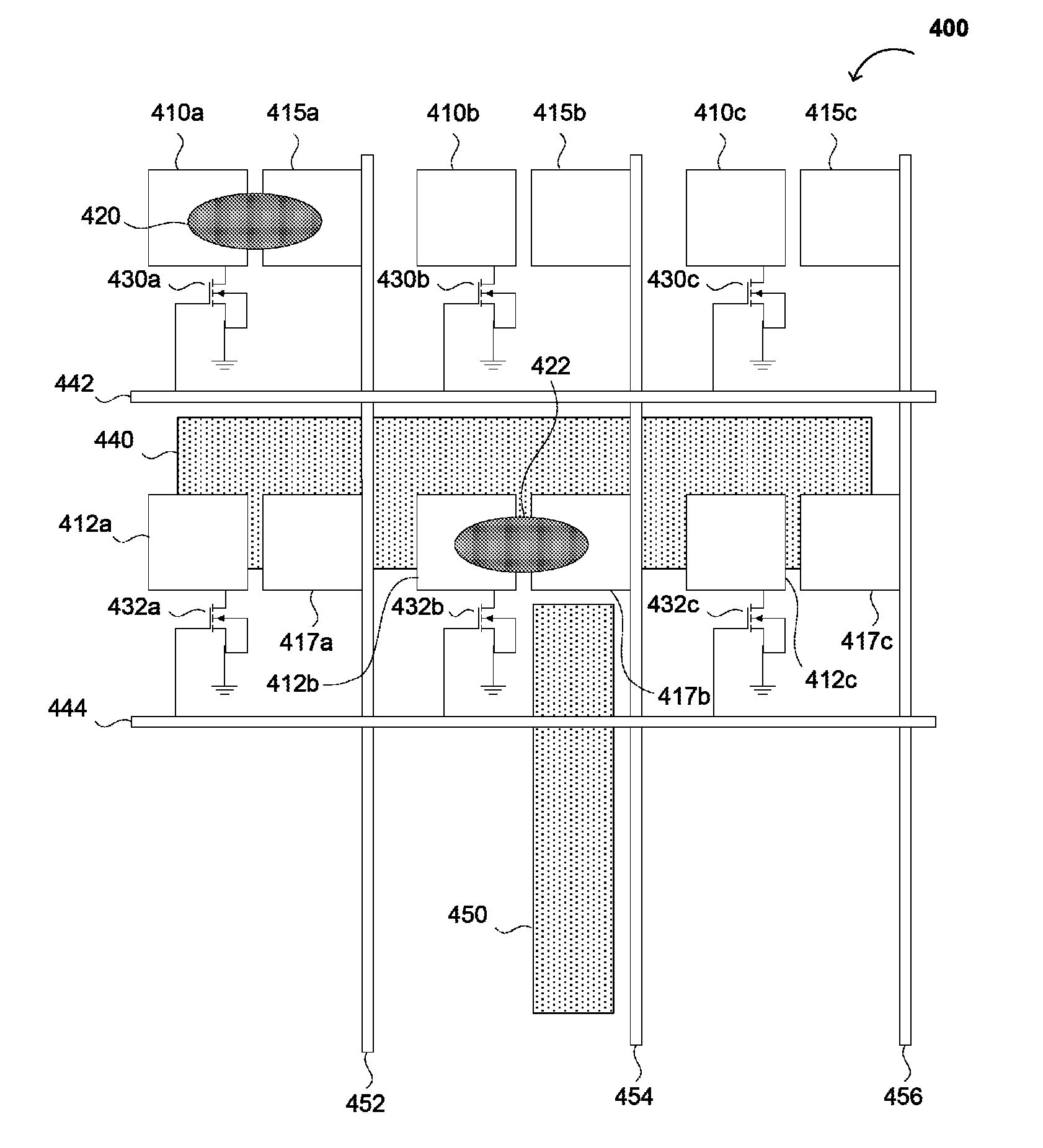
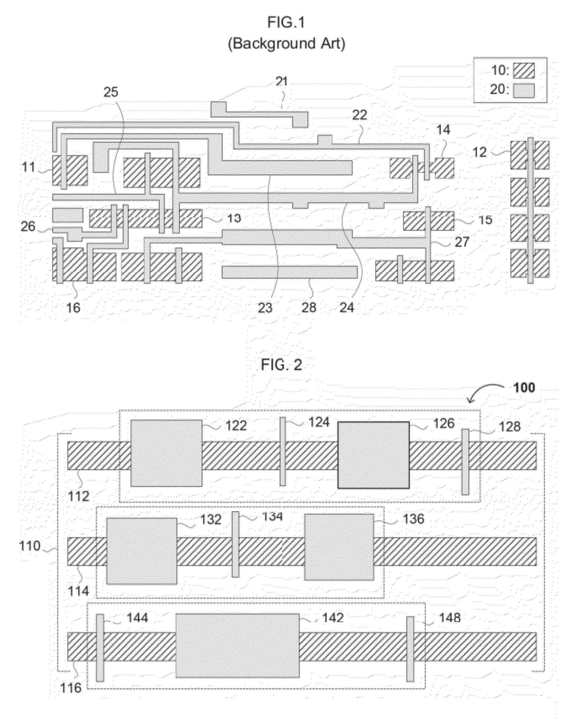
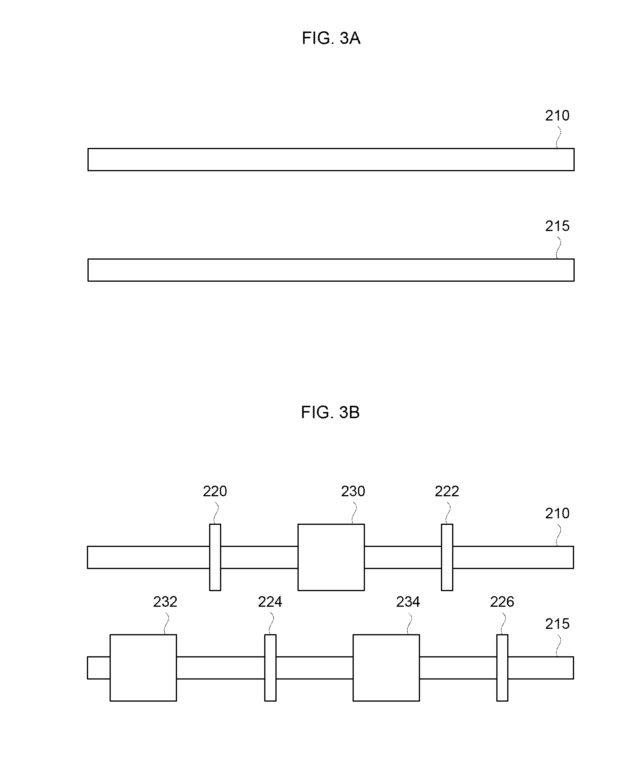
[0023]Reference will now be made in detail to various embodiments of the invention, examples of which are illustrated in the accompanying drawings. While the invention will be described in conjunction with exemplary embodiments, it will be understood that the description is not intended to limit the invention to these embodiments. On the contrary, the invention is intended to cover alternatives, modifications and equivalents that may be included within the spirit and scope of the invention as defined by the appended claims. Furthermore, in the following detailed description, numerous specific details are set forth in order to provide a thorough understanding of the present invention. However, it will be readily apparent to one skilled in the art that the present invention may be practiced without these specific details. In other instances, well-known methods, procedures, components, and circuits have not been described in detail so as not to unnecessarily obscure aspects of the pres...


PUM

PropertyMeasurementUnit
lengthaaaaaaaaaa
lengthaaaaaaaaaa
lengthaaaaaaaaaa

Abstract

Embodiments of the present invention relate to circuit layouts that are compatible with printing electronic inks, printed circuits formed by printing an electronic ink or a combination of printing and conventional blanket deposition and photolithography, and methods of forming circuits by printing electronic inks onto structures having print-compatible shapes. The layouts include features having (i) a print-compatible shape and (ii) an orientation that is either orthogonal or parallel to the orientation of every other feature in the layout.

Description

RELATED APPLICATIONS[0001]This application claims the benefit of U.S. Provisional Patent Application Nos. 61 / 231,643, filed Aug. 5, 2009, and 61 / 255,804, filed Oct. 28, 2009, each of which is incorporated by reference herein in its entirety.FIELD OF THE INVENTION[0002]The present invention generally relates to layouts for printed electronics, printed circuits incorporating or based on these layouts, and methods of using these layouts to form structures in a circuit. The printed circuits may include printed semiconductor, conductor, and / or dielectric structures alone or in combination with conventionally formed structures. The methods used to form the printed circuits include printing semiconductor, conductor, dielectric, and / or dopant inks on various substrates and / or structures in a pattern corresponding to such layouts.BACKGROUND[0003]Printed electronic circuits have certain manufacturing issues that are not necessarily similar to conventional circuit photolithographically defined...

Claims


Application Information

Patent Timeline
Patent Type & Authority Patents(United States)
IPC IPC(8): H05K1/00G06F17/50H05K3/12
CPCH01L23/5328H05K1/16H05K1/0296H05K3/0085H01L51/0022H01L2924/09701H05K3/125Y10T29/49155H01L2924/0002H05K2201/09245H01L2924/00G11C14/0054G11C17/14G11C17/18H10K71/611
Inventor WANG, ZHIGANGSUBRAMANIAN, VIVEKCLEVELAND, LEE
Owner ENSURGE MICROPOWER ASA
Why Eureka
Try Eureka