Semiconductor device and fabrication method thereof

a technology of semiconductor devices and manufacturing methods, which is applied in the direction of semiconductor devices, semiconductor/solid-state device details, electrical apparatus, etc., can solve the problems of poor electrical performance of the formed semiconductor devices and affect the electrical performance of the semiconductor devices, so as to improve the performance and yield of the ultimately formed semiconductor devices, improve the quality of the interconnection layer, and improve the quality of the ultimately formed source-drain plug layer

Pending Publication Date: 2022-03-10
SEMICON MFG INT (SHANGHAI) CORP +1
View PDF0 Cites 0 Cited by
  • Summary
  • Abstract
  • Description
  • Claims
  • Application Information

AI Technical Summary

Benefits of technology

[0026]The disclosed embodiments may have following beneficial effects. In the disclosed fabrication method of the present disclosure, an interface layer may be formed on the top surface of each of the source-drain plug layer and the gate structure. Therefore, the interface layers having same properties may be formed on the top surfaces of the source-drain plug layer and the gate structure. When subsequently forming the interconnection layers on the top surfaces of the source-drain plug layer and the gate structure, the rates of forming the interconnection layers over the source-drain plug layer and the gate structure may be consistent, which may avoid the formation of holes in the interconnection layer caused by the uneven growth rate, and may improve the quality of the formed interconnection layer. At the same time, because the interface layer is formed over the source-drain plug layer, the top surface of the source-drain plug layer may be sealed, which may prevent the source-drain plug layer from being damaged in subsequent processes, and may improve the quality of the ultimately formed source-drain plug layer, thereby improving the performance and yield of the ultimately formed semiconductor devices.
[0027]Further, the resistance of the interface layer may be less than the resistance of the barrier layer. When subsequently forming the interconnection layer over the interface layer, the interface layer may reduce the resistance at the bottom of each of the first through-hole and the second through-hole, thereby reducing the contact resistance (Rc) or sheet resistance (Rs) of the formed semiconductor device, and improving the electrical performance and use performance of the formed semiconductor device.
[0028]In the disclosed semiconductor device of the present disclosure, because the interface layer is disposed on each of the top surface of the source-drain plug layer exposed by the first through-hole and the top surface of the gate structure exposed by the second through-hole, the interface layers with same material properties may be formed on the top surfaces of the exposed source-drain plug layer and the exposed gate structure. In the process of subsequently forming the interconnection layers, the interconnection layers may be grown at the same environment, such that the interconnection layers on the top surfaces of the source-drain plug layer and the gate structure may have a same growth rate, which may avoid the formation of holes in the interconnection layer caused by uneven growth rate, and may improve the performance of the ultimately formed semiconductor device. At the same time, because the interface layer is formed over the source-drain plug layer, the top surface of the source-drain plug layer may be sealed, which may prevent the source-drain plug layer from being damaged in subsequent processes, and may improve the quality of the ultimately formed source-drain plug layer.
[0029]Further, the interface layer may be made of a metal alloy, such that the resistance at each of the top surface of the exposed source-drain plug layer and the top surface of the exposed gate structure may be reduced, thereby reducing the contact resistance (Rc) or sheet resistance (Rs) of the formed semiconductor device, and improving the electrical performance and use performance of the formed semiconductor device.

Problems solved by technology

A conventional planar transistor has substantially weak control ability on channel current, which causes a short channel effect and leads to a leakage current, and ultimately affects the electrical performance of the semiconductor device.
However, the formation qualities of the formed metal plug and the interconnection layer are poor, which causes poor electrical performance of the formed semiconductor device.
How to form high-quality metal plug and interconnection layer to ensure that the formed semiconductor device has desired performance is an urgent technical problem that needs to be solved.

Method used


Image

  • Semiconductor device and fabrication method thereof
  • Semiconductor device and fabrication method thereof

Examples


Embodiment Construction

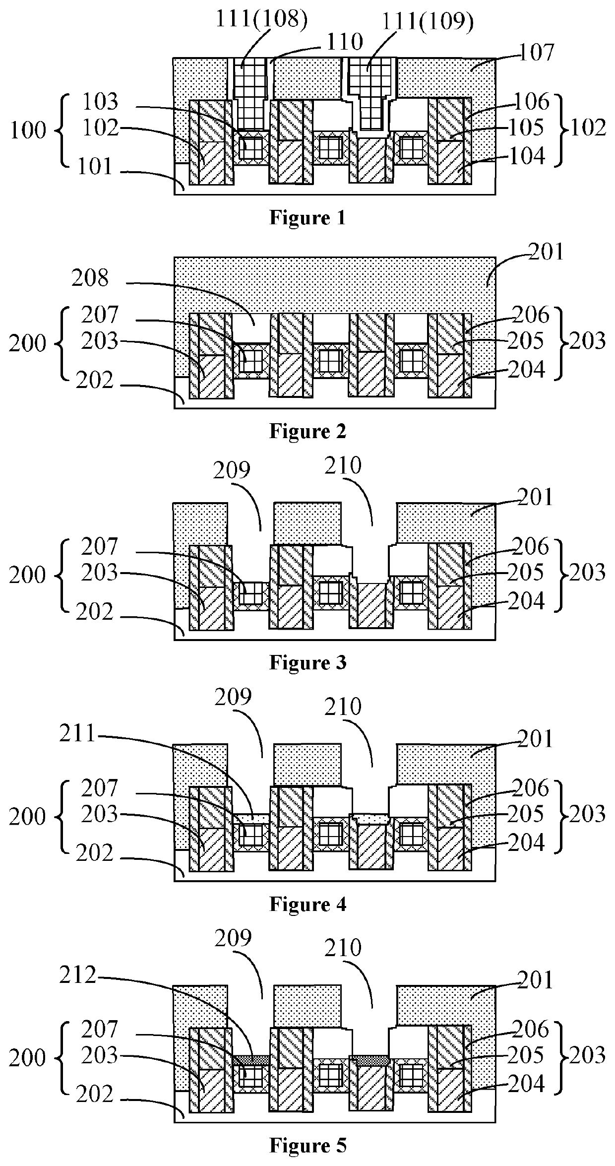
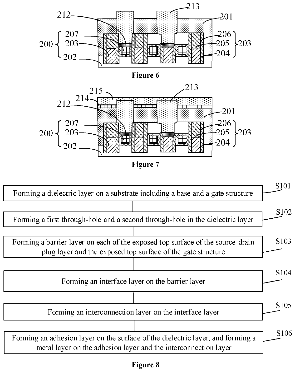
[0034]Reference will now be made in detail to exemplary embodiments of the disclosure, which are illustrated in the accompanying drawings. Wherever possible, the same reference numbers will be used throughout the drawings to refer to the same or the alike parts.

[0035]In a contact-over-active-gate (COAG) structure, an interconnection layer as a contact plug is formed over a source-drain plug layer and a gate structure, such that the source-drain plug layer and the gate structure are electrically connected to metal layers formed over the contact plug, respectively. The source-drain plug layer tends to be damaged in subsequent processes, and at the same time, a contact resistance (Rc) and a sheet resistance (Rs) of the formed semiconductor device are substantially large, which affects the electrical performance and usability of the semiconductor device, and limits the application of the semiconductor device.

[0036]Referring to FIG. 1, the semiconductor device includes a substrate 100. T...


PUM

PropertyMeasurementUnit
dielectric constantaaaaaaaaaa
temperatureaaaaaaaaaa
resistanceaaaaaaaaaa

Abstract

A semiconductor device and a fabrication method of the semiconductor device are provided. The semiconductor device includes a substrate, a source-drain plug layer in the substrate, a gate structure in the substrate, and a dielectric layer disposed over the substrate and covering the gate structure and the source-drain plug layer. The dielectric layer contains a first through-hole having a bottom exposing a top surface of the source-drain plug layer, and a second through-hole having a bottom exposing a top surface of the gate structure. Further, the semiconductor device includes an interface layer disposed on each of the top surface of the source-drain plug layer exposed by the first through-hole and the top surface of the gate structure exposed by the second through-hole.

Description

CROSS-REFERENCES TO RELATED APPLICATIONS[0001]This application claims the priority of Chinese patent application No. 202010942616.6, filed on Sep. 9, 2020, the entirety of which is incorporated herein by reference.FIELD OF THE DISCLOSURE[0002]The present disclosure generally relates to the field of semiconductor manufacturing technology and, more particularly, relates to a semiconductor device and a fabrication method thereof.BACKGROUND[0003]With the rapid development of semiconductor manufacturing technology, semiconductor devices have been developed towards with higher component density and higher integration degree. As the most basic semiconductor device, transistors have been widely used currently. A conventional planar transistor has substantially weak control ability on channel current, which causes a short channel effect and leads to a leakage current, and ultimately affects the electrical performance of the semiconductor device.[0004]In a manufacturing process of the semicon...

Claims


Application Information

Patent Timeline
Patent Type & Authority Applications(United States)
IPC IPC(8): H01L21/768H01L23/522H01L23/532
CPCH01L21/76858H01L21/76877H01L21/76843H01L23/5226H01L21/76802H01L23/53252H01L23/53266H01L23/53209H01L23/53238H01L23/5384H01L23/5386H01L23/5283H01L23/5286H01L23/53261H01L21/76831H01L21/76847H01L21/76879H01L21/76897
Inventor ZHANG, TIANTIANJING, XUEZHEN
Owner SEMICON MFG INT (SHANGHAI) CORP
Why Eureka
Try Eureka