Radiofrequency high-output device

a high-output, radiofrequency technology, applied in semiconductor devices, semiconductor/solid-state device details, electrical apparatus, etc., can solve the problems of large cost of such work, and mismatch in linear expansion coefficient, so as to prevent cracks or breakages in component parts

Active Publication Date: 2017-06-20
MITSUBISHI ELECTRIC CORP
View PDF12 Cites 0 Cited by
  • Summary
  • Abstract
  • Description
  • Claims
  • Application Information

AI Technical Summary

Benefits of technology

[0009]In view of the above-described problem, an object of the present invention is to provide a radiofrequency high-output device capable of preventing cracks or breakages in component parts when the device is mounted (secondarily mounted) on a customer's circuit board.
[0011]In the present invention, the groove is provided between the mount portion and the flange portions of the base plate. Therefore, when the base plate warped due to an initial warp of the package or mounting of the semiconductor chips and the matching circuit substrates is fixed on the aluminum heat sink plate on the circuit board with the screw, only the flange portions can easily be bent starting from the groove so that stress caused in the mount portion at the time of correcting the warp is reduced. Consequently, when the radiofrequency high-output device is mounted (secondarily mounted) on the customer's circuit board, stresses caused in the semiconductor chips and other component parts mounted on the mount portion of the base plate can be reduced to prevent cracks or breakages in the component parts.

Problems solved by technology

Also, after the semiconductor chips and the matching circuit substrates are mounted with solder, complicated warps result due to a mismatch in linear expansion coefficient between the these component parts.
When the device is mounted on the aluminum heat sink plate on the customer's circuit board with screws while having such warps, the warps are corrected but stresses caused in the semiconductor chips and the matching circuit substrates are increased, resulting in cracks or breakages in the component parts.
However, the cost of such working is considerably high.
However, this technique is not effective in solving the above-mentioned problem with fixing of the base plate with screws.

Method used


Image

  • Radiofrequency high-output device
  • Radiofrequency high-output device
  • Radiofrequency high-output device

Examples


first embodiment

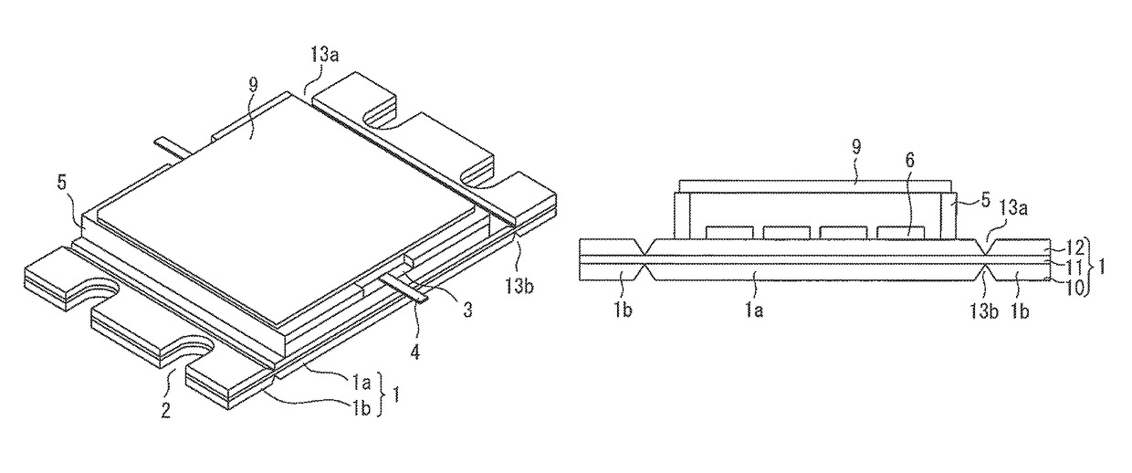
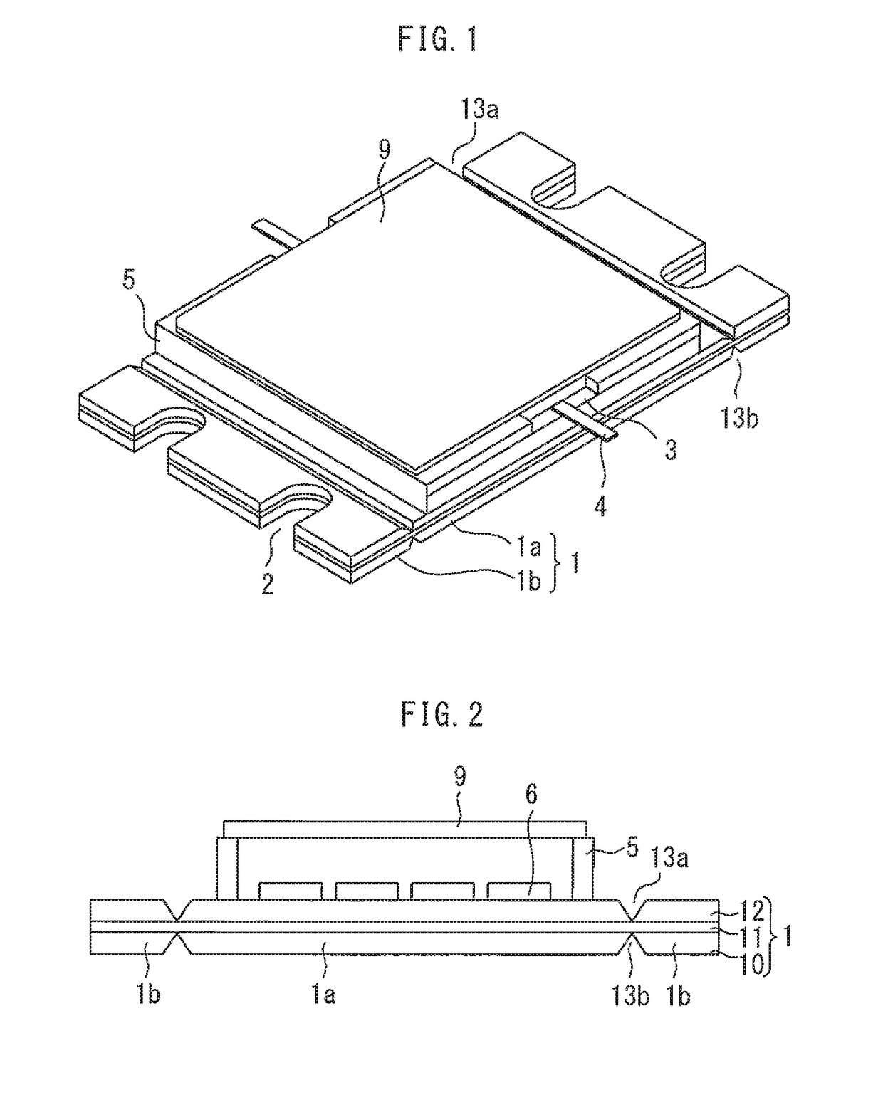
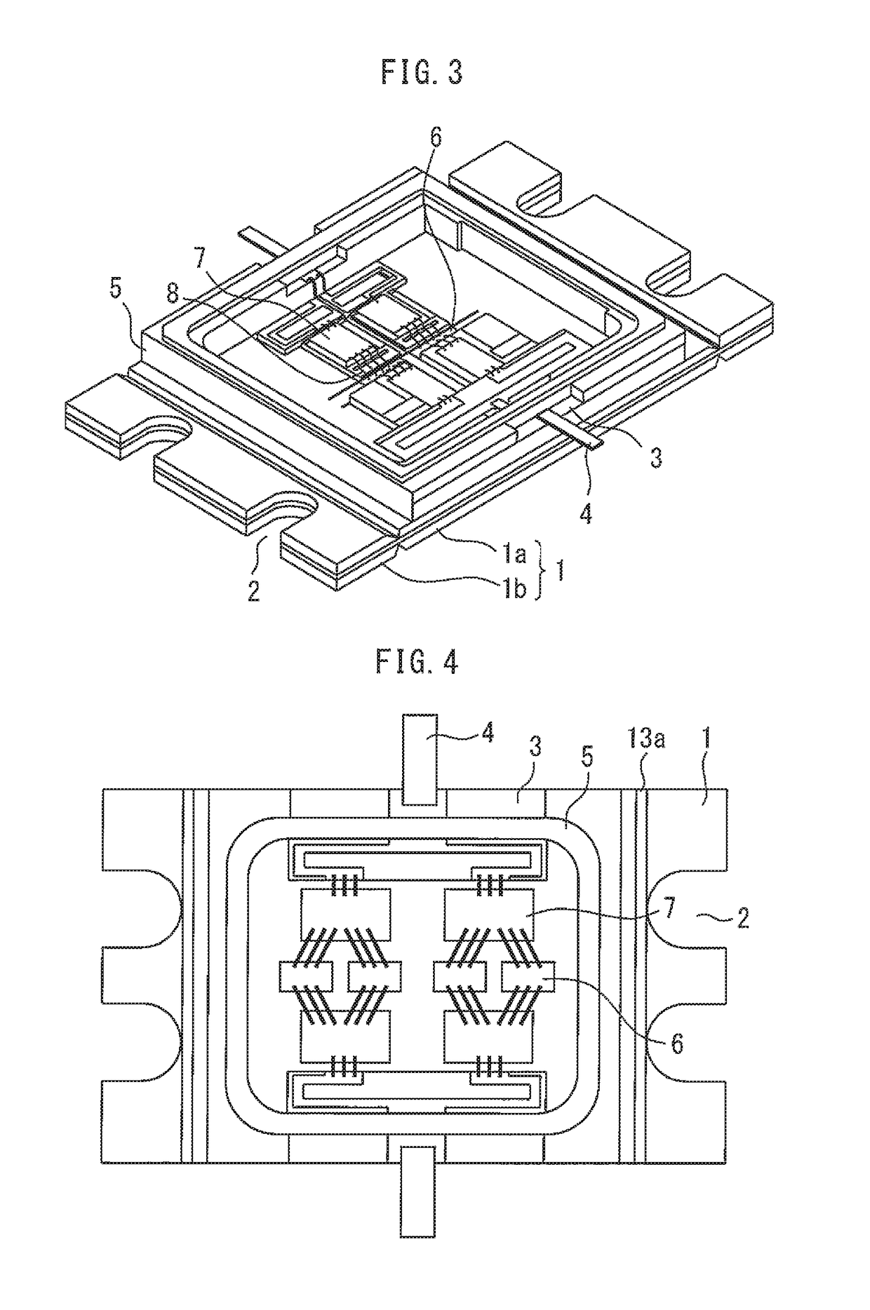
[0027]FIGS. 1 and 2 are a perspective view and a sectional view, respectively, of a radiofrequency high-output device according to a first embodiment of the present invention. FIGS. 3 and 4 are a perspective view and a sectional view each showing internal portions of the radiofrequency high-output device according to the first embodiment of the present invention.

[0028]A base plate 1 has a mount portion 1a and flange portions 1b. The mount portion 1a is disposed at a center of the base plate 1 in a direction along longer sides of the base plate 1, and the flange portions 1b are disposed on opposite sides of the mount portion 1a. Cuts 2 in which screws are inserted to fix the base plate 1 are provided in the flange portions 1b. In this embodiment, the cut 2 is provided in at least one place at each of the opposite shorter sides of the base plate 1. An aperture may be provided in place of the cut 2.

[0029]On an upper surface of the mount portion 1a of the base plate 1, ceramic terminals...

second embodiment

[0037]FIG. 9 is a sectional view of a radiofrequency high-output device according to a second embodiment of the present invention. In the second embodiment, V-grooves 13a are provided only in the upper surface of the base plate 1 between the mount portion 1a and the flange portions 1b of the base plate 1. The V-grooves 13a are provided in the Cu plate 12. The depths of the V-grooves 13a may be such that the V-grooves 13a reach or do not reach the Mo plate 11. The V-grooves 13a may have U-shaped cross sections or certain recessed cross sections. The shapes of the V-grooves 13a are not specially specified. The flange portions 1b are enabled to bend easily starting from the V-grooves 13a. An effect similar to that in the first embodiment can thus be obtained.

third embodiment

[0038]FIG. 10 is a sectional view of a radiofrequency high-output device according to a third embodiment of the present invention. In the third embodiment, V-grooves 13a and 13b are provided in positions not corresponding to each other in the vertical direction in the upper and lower surfaces of the base plate 1 between the mount portion 1a and the flange portions 1b of the base plate 1. The V-grooves 13a and 13b are provided in the Cu plates 12 and 10, respectively. The depths of the V-grooves 13a and 13b may be such that the V-grooves 13a and 13b reach or do not reach the Mo plate 11. The V-grooves 13a and 13b may have U-shaped cross sections or certain recessed cross sections. The shapes of the V-grooves 13a and 13b are not specially specified.

[0039]The flange portions 1b are enabled to bend easily starting from the V-grooves 13a and 13b. An effect similar to that in the first embodiment can thus be obtained. The provision of the V-grooves 13a and 13b in positions not correspondi...


PUM


Abstract

A radiofrequency high-output device includes: a base plate having a mount portion and a flange portion; a frame joined to an upper surface of the mount portion; and a semiconductor chip mounted on the upper surface of the mount portion in the frame, wherein a cut or an aperture in which a screw is inserted to fix the base plate is provided in the flange portion, and a groove is provided between the mount portion and the flange portion of the base plate.

Description

BACKGROUND OF THE INVENTION[0001]Field of the Invention[0002]The present invention relates to a radiofrequency high-output device.[0003]Background Art[0004]In a radiofrequency high-output device, terminals and a frame are brazed on a base plate, and semiconductor chips and matching circuit substrates are mounted in the frame on the base plate. A frame upper surface is covered with a cap to hermetically enclose the interior of the frame.[0005]A CuW member, a Cu—Mo alloy member, a Cu—Mo—Cu multilayer member or the like is used as the base plate by considering heat dissipation from the semiconductor chips and matching in linear expansion coefficient between the semiconductor chips and the base plate. Schemes to develop semiconductor chips of higher outputs have recently been advanced and Cu—Mo—Cu multilayer members having a high heat dissipation characteristic are therefore used.[0006]The base plate has cuts provided at each of its opposite shorter sides. The radiofrequency high-output...

Claims


Application Information

Patent Timeline
Patent Type & Authority Patents(United States)
IPC IPC(8): H01L23/10H01L23/043H01L21/48H01L23/34H01L23/373H01L23/13H01L23/14H01L23/40H01L23/492
CPCH01L23/3736H01L21/4803H01L23/043H01L23/13H01L23/142H01L23/4006H01L23/492H01L2224/48091H01L2224/49111H01L2224/291H01L2224/2919H01L24/48H01L24/49H01L2224/45144H01L2224/48157H01L23/66H01L2224/49175H01L24/45H01L24/29H01L2224/32245H01L24/32H01L23/562H01L2924/00014H01L2924/014
Inventor MIYAWAKI, KATSUMINISHIHARA, TATSUTO
Owner MITSUBISHI ELECTRIC CORP
Why Eureka
Try Eureka