Perforation of films for separation

a technology of perforation and film, applied in the direction of semiconductor devices, semiconductor/solid-state device details, electrical devices, etc., can solve the problems of subsequent cell-level handling and processing of expensive additional tooling, and achieve the effects of high reliability of cutting and separation process, easy pulling apart, and balanced holding strength

Active Publication Date: 2018-01-02
ALTA DEVICES INC
View PDF24 Cites 0 Cited by
  • Summary
  • Abstract
  • Description
  • Claims
  • Application Information

AI Technical Summary

Benefits of technology

[0005]We describe a method for keeping cut cells in place and oriented within the tile's original geometry. A physical, final separation of cells from one another follows at a later time. The method would include leaving strategic material intact during cutting by skipping certain sections during the cut and leaving specific geometry of material (“tabs”) that would easily pull apart. The individual cells are kept in their respective positions by the tabs during manufacturing processes such as testing, handling, and inventory control, prior to final separation. The tabs provide structural support so that the cut cells do not fall out of alignment from their original geometry, and can still be handled as a single tile-unit. The number, placement, and geometry of these tabs are optimized to balance holding strength with the need to eventually physically separate the selected cells by breaking or cutting those tabs.
[0006]This invention allows: a highly reliable cutting and separation process; simplified testing of individual cells; cell test AFTER cutting; convenient storage / inventory buildup of films after cutting and testing, but prior to separation; reliable tile-level handling along the manufacturing line; controllable and consistent separation force; selectivity of areas / geometry to be subjected to separation forces / stresses; and spatial control of cell support points prior to final separation (optimize end effector during robot handling).

Problems solved by technology

Such existing approaches utilizing fully-separated cells require expensive additional tooling for subsequent cell-level handling and processing.

Method used


Image

  • Perforation of films for separation
  • Perforation of films for separation
  • Perforation of films for separation

Examples


Embodiment Construction

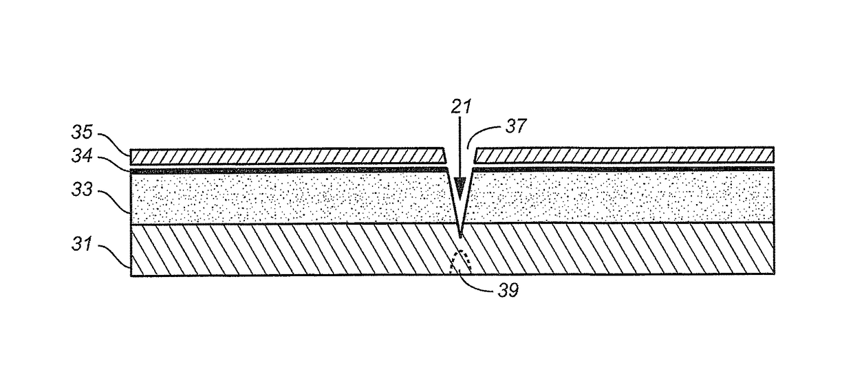
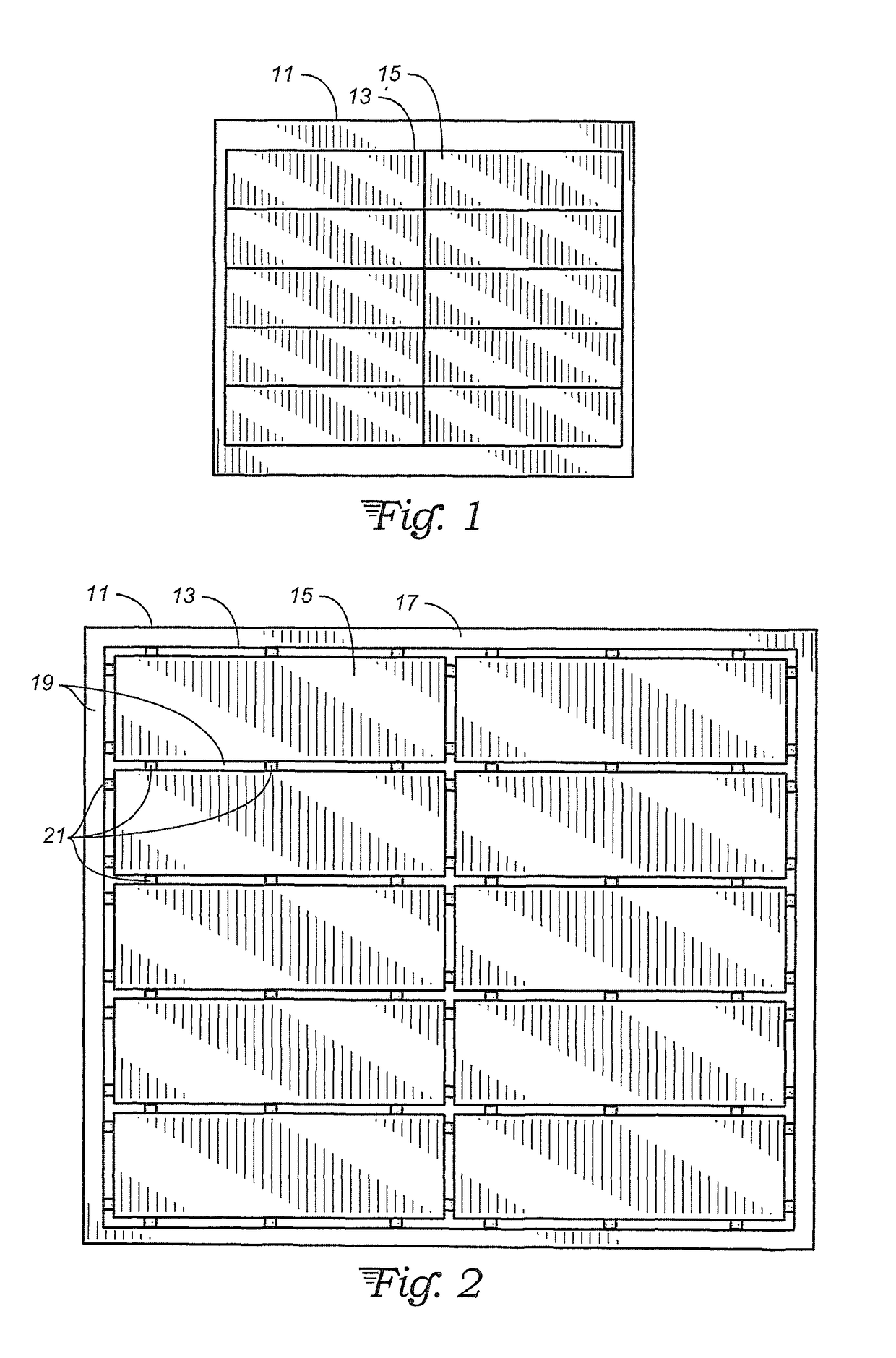
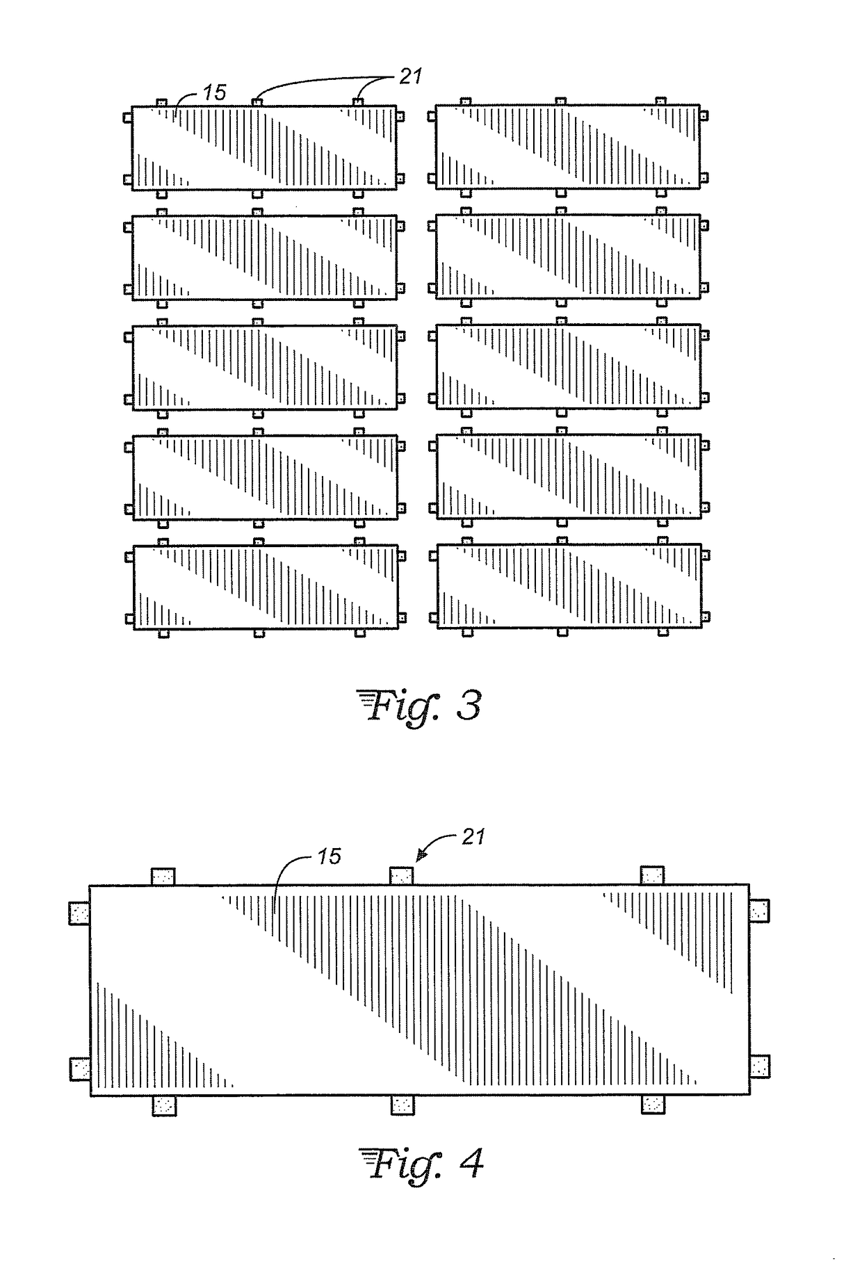
[0012]With reference to FIG. 1, a film of material on a frame assembly 11 is seen in its state prior to any laser or mechanical separation. As seen in FIG. 5, tiles 13 may be a multi-layer composite of a thin semiconductor film 35, approximately 1 to 20 microns thick, that is supported by a polymer sheet 31, such as one composed of polyethylene terephthalate (PET), approximately 25 to 100 microns thick. A copper base 34 of the semiconductor film 35 may be bonded to the PET sheet 31 by an approximately 25 to 100 micron thick layer of an adhesive (PSA) 33. Returning to FIG. 1, tiles of material 13, e.g. of approximately 100 mm×100 mm size, can be created this way and patterned with a number of individual cells 15. The individual cells 15 must ultimately be separated from one another in order to sort them according to quality. A repeatable, accurate, fast, low cost method to free (separate) the cells would be very attractive.

[0013]With reference to FIG. 2, the method would include the ...


PUM


Abstract

A method for separation of semiconductor device cell units from fabricated large-area cell units, together with a corresponding tile unit structure, are provided in which the tile unit is cut along cell unit boundaries while leaving intact a set of specified tab sections distributed along the cell unit boundaries. The tile unit may be a multi-layer composite of a semiconductor layer with a conductive metallic base supported upon a polymer layer and adhered thereto by an adhesive film, wherein tab sections are cut completely through the semiconductor layer and its metallic base from above and may also be cut partially through the polymer layer from below, leaving at least a portion of the polymer layer in place at tab sections. Tile units can be handled such that component cell units are held together by the tab sections, until a physical final separation of selected cell units.

Description

CROSS-REFERENCE TO RELATED APPLICATION[0001]This application claims priority under 35 U.S.C. 119(e) from prior U.S. provisional application 62 / 049,227, filed Sep. 11, 2014.TECHNICAL FIELD[0002]The invention relates to preparation of fabricated arrays of semiconductor devices for subsequent testing and handling, and in particular to arrangements for separating individual semiconductor devices from such arrays.BACKGROUND ART[0003]The process for creating semiconductor thin-film optoelectronic devices involves fabrication of relatively large-area units, or “tiles,” which are then separated into smaller units, or “cells.” Instruments used for this separation include mechanical cutting tools and lasers. These instruments take “tiles” and produce “cells”, with no intermediate state. Such existing approaches utilizing fully-separated cells require expensive additional tooling for subsequent cell-level handling and processing.[0004]There can be processing advantages to having a technique wh...

Claims


Application Information

Patent Timeline
Patent Type & Authority Patents(United States)
IPC IPC(8): H01L21/00H01L21/78H01L23/00
CPCH01L21/78H01L23/562H01L2924/0002H01L2924/00
Inventor SORABJI, KHURSHEDPATTERSON, DANIEL G.
Owner ALTA DEVICES INC
Why Eureka
Try Eureka