Pixel circuit, driving method thereof and display device

a technology of pixel circuit and display device, applied in the direction of instruments, static indicating devices, etc., can solve the problems of insufficient brightness of white display, insufficient electric current, and instant reduction of electric current, and achieve the effect of preventing contrast deterioration

Active Publication Date: 2018-02-13
TIANMA MICRO ELECTRONICS CO LTD +1
View PDF6 Cites 1 Cited by
  • Summary
  • Abstract
  • Description
  • Claims
  • Application Information

AI Technical Summary

Benefits of technology

[0019]As an exemplary advantage according to the invention, the present invention is designed to include a current detour transistor for allowing the electric current supplied from the driving transistor to be detoured to the reference voltage power supply line without going through the light emitting element. Therefore, it is possible to prevent contrast deterioration caused by leaked light emission at the time of reset actions through turning on the current detour transistor at the time of the reset actions.

Problems solved by technology

However, there are following issues with the existing pixel circuit having the threshold voltage detecting function.
(1) Leaked light emission at the time of a reset action causes contrast deterioration.
(2) Due to the hysteresis characteristic of the driving transistor, several frames are required to completely change the black image to the white image even though the image data has been already completely re-written from black to white.
Thus, even when a white-display Vgs bias determined based on the initialized hysteresis characteristic is applied, the electric current is instantly decreased by the hysteresis characteristic for lighting up so that it is insufficient for providing the original brightness of white display.
(3) The threshold voltage detection period is limited to one horizontal scanning period, so that the compensation accuracy of the threshold voltage becomes deteriorated when the display resolution becomes higher.
Thereby, detection accuracy of the threshold voltage is deteriorated, so that compensation accuracy of the threshold voltage is worsened as well.

Method used


Image

  • Pixel circuit, driving method thereof and display device
  • Pixel circuit, driving method thereof and display device
  • Pixel circuit, driving method thereof and display device

Examples


first exemplary embodiment

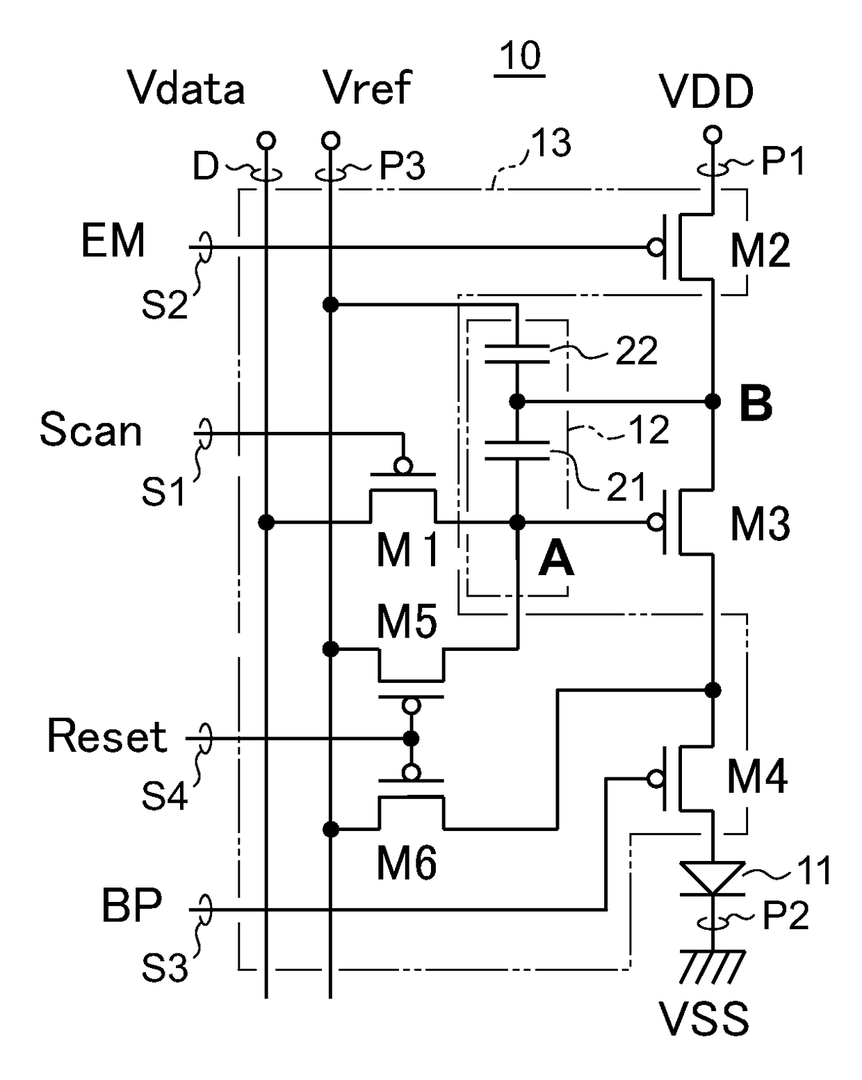
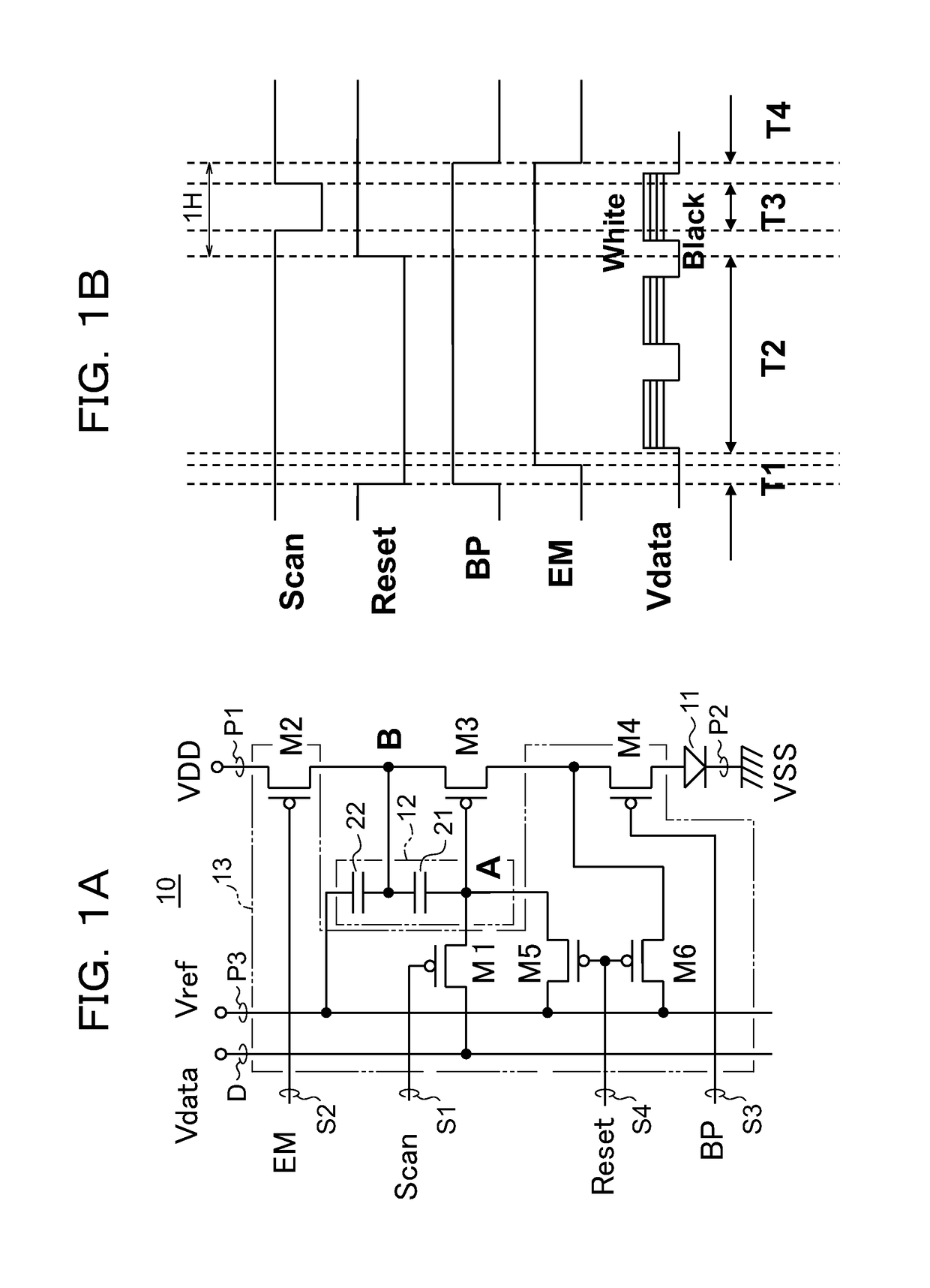
[0038]FIG. 1A is a circuit diagram showing the structure of a pixel circuit according to a first exemplary embodiment, and FIG. 1B is a timing chart showing actions of the pixel circuit of the first exemplary embodiment. Explanations will be provided hereinafter by referring to those drawings.

[0039]A pixel circuit 10 of the first exemplary embodiment includes: a light emitting element 11; a driving transistor (M3) which supplies an electric current to the light emitting element 11 according to an applied voltage; a capacitor part 12 which holds a voltage containing a threshold voltage Vth and a data voltage Vdata of the driving transistor (M3) and applies the voltage to the driving transistor (M3); and a switch part 13 which makes the capacitor part 12 hold the voltage containing the threshold voltage Vth and the data voltage Vdata. Further, the switch part 13 includes a current detour transistor (M6) which makes the electric current supplied from the driving transistor (M3) detour ...

second exemplary embodiment

[0104]FIG. 8A is a circuit diagram showing a part of a display device according to a second exemplary embodiment, and FIG. 8B is a timing chart showing actions of the display device according to the second exemplary embodiment. Explanations will be provided hereinafter by referring to those drawings.

[0105]The display device of the second exemplary embodiment exhibits a specific feature in its de-multiplexer 134. The de-multiplexer 134 shown in FIG. 8A is for one pixel. In a case where the pixel circuit of the first exemplary embodiment is a sub-pixel, a single pixel is constituted with three sub-pixels of R (Red), G (Green) and B (Blue). Each of the pixel circuits is in an RGB vertical stripe layout structure, for example.

[0106]The de-multiplexer 134 selects one data line sequentially from three data lines Dnr, Dng, and Dnb each being connected to three respective pixel circuits, and connects the selected single data line to another single data line Dn that is connected to a supply ...


PUM


Abstract

To provide a pixel circuit and the like capable of preventing contrast deterioration caused by leaked light emission at the time of reset actions. The pixel circuit includes: a light emitting element; a driving transistor which supplies an electric current to the light emitting element according to an applied voltage; a capacitor part which holds a voltage containing a threshold voltage and a data voltage of the driving transistor and applies the voltage to the driving transistor; and a switch part which makes the capacitor part hold the voltage containing the threshold voltage and the data voltage. The switch part includes a current detour transistor which makes the electric current supplied from the driving transistor detour to a reference voltage power supply line without going through the light emitting element.

Description

CROSS-REFERENCE TO RELATED APPLICATION[0001]This application is based upon and claims the benefit of priority from Japanese patent application No. 2014-206933, filed on Oct. 8, 2014, the disclosure of which is incorporated herein in its entirety by reference.BACKGROUND OF THE INVENTION[0002]1. Field of the Invention[0003]The present invention relates to a pixel circuit used in an Active Matrix Organic Emitting Light Display (referred to as “AMOLED Display” hereinafter) and the like, a driving method thereof, and a display device which is provided with the pixel circuit. While an organic light emitting diode is also referred to as an organic EL element, it is referred hereinafter as “OLED (Organic Light Emitting Diode)”.[0004]2. Description of the Related Art[0005]There is no standard pixel circuit of AMOLED display, so that each of the companies manufacturing AMOLED display uses their original pixel circuits. Hereinafter, a basic pixel circuit will be described. FIG. 9A is a circuit...

Claims


Application Information

Patent Timeline
Patent Type & Authority Patents(United States)
IPC IPC(8): G09G3/32G09G3/3233G09G3/20
CPCG09G3/3233G09G2300/0852G09G2310/0262G09G2310/0251G09G2300/0861
Inventor MATSUEDA, YOJIRONONAKA, YOSHIHIROTAKATORI, KENICHI
Owner TIANMA MICRO ELECTRONICS CO LTD
Why Eureka
Try Eureka