Semiconductor modules and manufacture method thereof

A semiconductor and integrated technology, applied in semiconductor/solid-state device manufacturing, semiconductor devices, semiconductor/solid-state device components, etc., can solve problems such as difficult to clean gaps

Inactive Publication Date: 2008-08-06
SANYO ELECTRIC CO LTD
View PDF10 Cites 0 Cited by
  • Summary
  • Abstract
  • Description
  • Claims
  • Application Information

AI Technical Summary

Problems solved by technology

In this case, the connecting means such as solder formed between the lead wire 122 and the conductive pattern 132 is formed very thin, and the gap between the island 137 and the second PI sheet 134 is very narrow, so it is difficult to clean the gap.

Method used


Image

  • Semiconductor modules and manufacture method thereof
  • Semiconductor modules and manufacture method thereof
  • Semiconductor modules and manufacture method thereof

Examples


no. 1 example

[0079] As this apparatus, explain again what was explained in the prior art column Figure 25 hard drive 100.

[0080] In order to mount the hard disk 100 in a computer or the like, it is mounted on a motherboard 112 as necessary. The motherboard 112 is fitted with female (or male) connectors. The connector on the motherboard 112 is connected to the male (or female) connector 111 installed on the FCA and exposed from the back of the case 101 . In the case 101, the recording medium, that is, the recording disc 102 is stacked according to its capacity, and the magnetic head 104 floats above the recording disc 102 at a height of 20 to 30 nm. In order to scan, the interval between the recording discs 102 is set. If no problem occurs during the scanning, the recording disc 102 is mounted on the spindle motor 103 at this interval. The spindle motor 103 is mounted on a mounting substrate, and a connector disposed on the rear surface of the mounting substrate is exposed from the rea...

no. 4 example

[0119] Figure 7 In the semiconductor device 10B shown in A, the metal plate 23 is adhered to the Figure 6 shown on the semiconductor device 10A. Therefore, except for the metal plate 23 and Figure 6 Basically the same, the different parts are explained below.

[0120] Reference numeral 28 is a bonding device, which is also exposed from the solder pad 21 and the island 15 as can be seen from the manufacturing method described later. The exposed amount of the back surface of the metal plate 23 can be easily adjusted by the thickness of the metal plate. For example, when the solder 22 is melted, the metal plate 23 is pressed into the back of the bonding device 28, so that the thickness of the solder between the metal plate 23 and the island 15 can be determined as the protrusion amount of the bonding device 28.

[0121] Therefore, if the thickness of the metal plate 23 is determined, it is possible to calculate how much the back surface of the metal plate 23 protrudes from...

no. 6 example

[0127] Figure 8 The semiconductor device 10D shown in A is omitted Figure 6 , Figure 7 The island 15 is shown. exist Figure 17 In the process, if the region that becomes the island 15 is also removed, the back surface of the semiconductor element 16 is exposed from the insulating resin 25, and the back surface of the semiconductor element 16 is substantially on the same plane as the back surface of the solder pad 21. structure at the position.

[0128] In this case, it is possible to dispose the surface of the semiconductor element 16 at a ratio Figure 6 , Figure 7 The surface of the semiconductor element 16 is shown further below. Therefore, the top of the thin metal wire 26 can be positioned downward, the thickness of the insulating resin 25 can be reduced, and the overall size can also be reduced.

[0129] In addition to this feature, it is essentially the same as Figure 6 are the same, so the rest of the description is omitted.


PUM

PropertyMeasurementUnit
Thicknessaaaaaaaaaa

Abstract

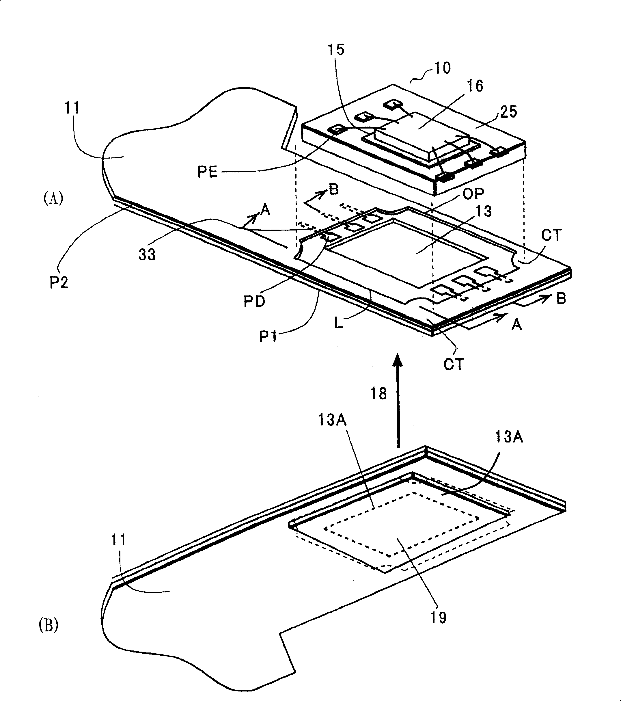
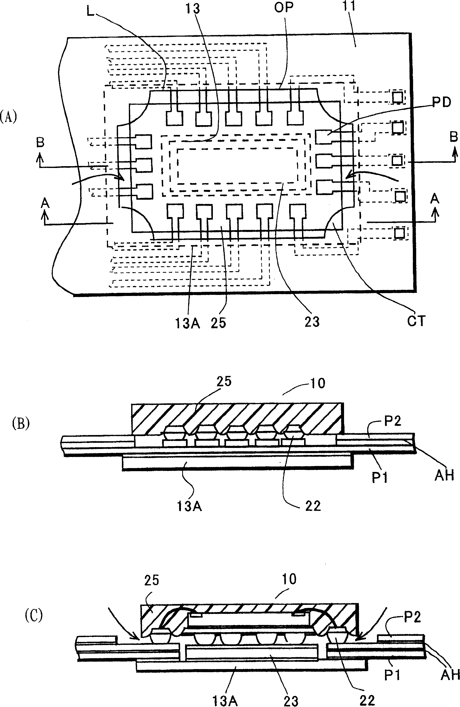
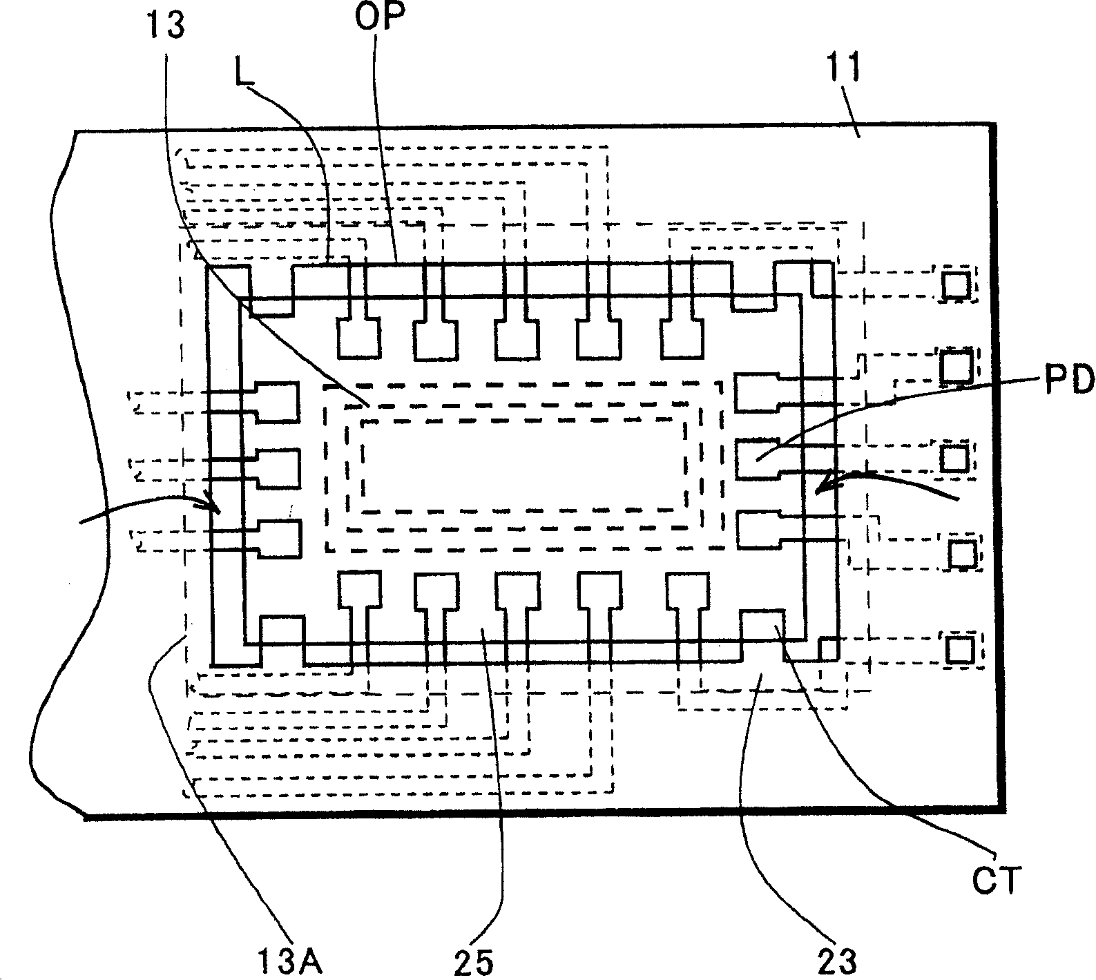
A first metal film 14 made of a Cu plated film is formed on a radiation substrate 13A made of A1, and an island 15 exposed from a back surface of a semiconductor device 10 is adhered thereto. At that time, the back surface of the semiconductor device 10 is brought into contact with contact areas, and a first opening portion OP is opened larger than an arranging area of the semiconductor device 10. Accordingly, the cleaning can be executed via the first opening portion OP exposed from peripheries of the semiconductor device 10. In addition, the heat generated from semiconductor elements 16 can be radiated excellently from the island 15 via a second supporting member 13A.

Description

technical field [0001] The present invention relates to a semiconductor device and a semiconductor module, and particularly to a structure capable of satisfactorily dissipating heat from a semiconductor element. Background technique [0002] In recent years, as semiconductor devices are used in portable equipment or small-sized, high-density mounting equipment, semiconductor devices that are light, thin, and good in heat dissipation are required. However, semiconductor devices are mounted on various substrates, and semiconductor modules contained in such substrates are mounted in various devices. The substrate may be a ceramic substrate, a printed substrate, a flexible sheet, a metal substrate, a glass substrate, or the like, and here, an example thereof will be described below as a semiconductor module mounted on a flexible sheet. It goes without saying that these substrates can also be used in this embodiment. [0003] Figure 25 A case where a semiconductor module using...

Claims


Application Information

Patent Timeline
IPC IPC(8): H01L23/48H01L23/12H01L21/60H05K1/00H01L21/48H01L23/29H01L23/36H01L23/40H01L23/433H05K1/02H05K1/18H05K3/26H05K3/28H05K3/30
CPCH05K3/303H01L2924/01046H01L2924/01082H01L2924/01004H05K1/182H05K3/26H05K1/189H01L2224/32245H01L2224/16H05K1/021H01L2924/15311H01L2924/01029H05K1/0204H01L2924/0132H05K3/281H05K2201/10416H01L2224/48091H01L2224/16245H01L2224/49171H01L2924/01013H01L24/32H01L2224/92247H01L2924/0103H01L2224/32057H01L2924/3011H01L2924/01047H01L2924/1433H01L2924/01079H01L24/48H01L2224/83385H01L2224/48465H05K2201/10734H01L2224/48247H05K2201/2036H01L23/36H01L23/4334H01L2924/01033H01L2924/01005H01L2924/01006H01L24/49H01L2924/01059H01L2924/01078H05K2201/10727H01L2224/73265H01L2924/12044H01L21/4832H01L2924/07802H01L24/97H01L2224/97H01L2224/451H01L2924/351H01L2924/15787H01L2924/12042H01L24/45H01L24/73H01L2224/05571H01L2224/05573H01L2924/00014H01L2924/181H01L2224/73257H01L2924/1815H01L2924/18165H01L2224/06135Y02P70/50H01L2924/00H01L2924/00012H01L2924/01026H01L2924/01028H01L2224/83H01L2224/85H01L2224/05599
Inventor 坂本则明小林义幸阪本纯次冈田幸夫五十岚优助前原荣寿高桥幸嗣
Owner SANYO ELECTRIC CO LTD
Why Eureka
Try Eureka