
Manufacturing method and structure of organic luminous display panel

A technology for luminescent display and manufacturing method, which is applied in the direction of electroluminescent light source, semiconductor/solid-state device manufacturing, light source, etc. It can solve the problems of bright lines and high brightness of finished panel products, and achieve the effect of improving the problem of bright lines

Inactive Publication Date: 2008-08-13
TECO ELECTRIC AND MACHINERY
View PDF1 Cites 0 Cited by
  • Summary
  • Abstract
  • Description
  • Claims
  • Application Information

AI Technical Summary

Problems solved by technology

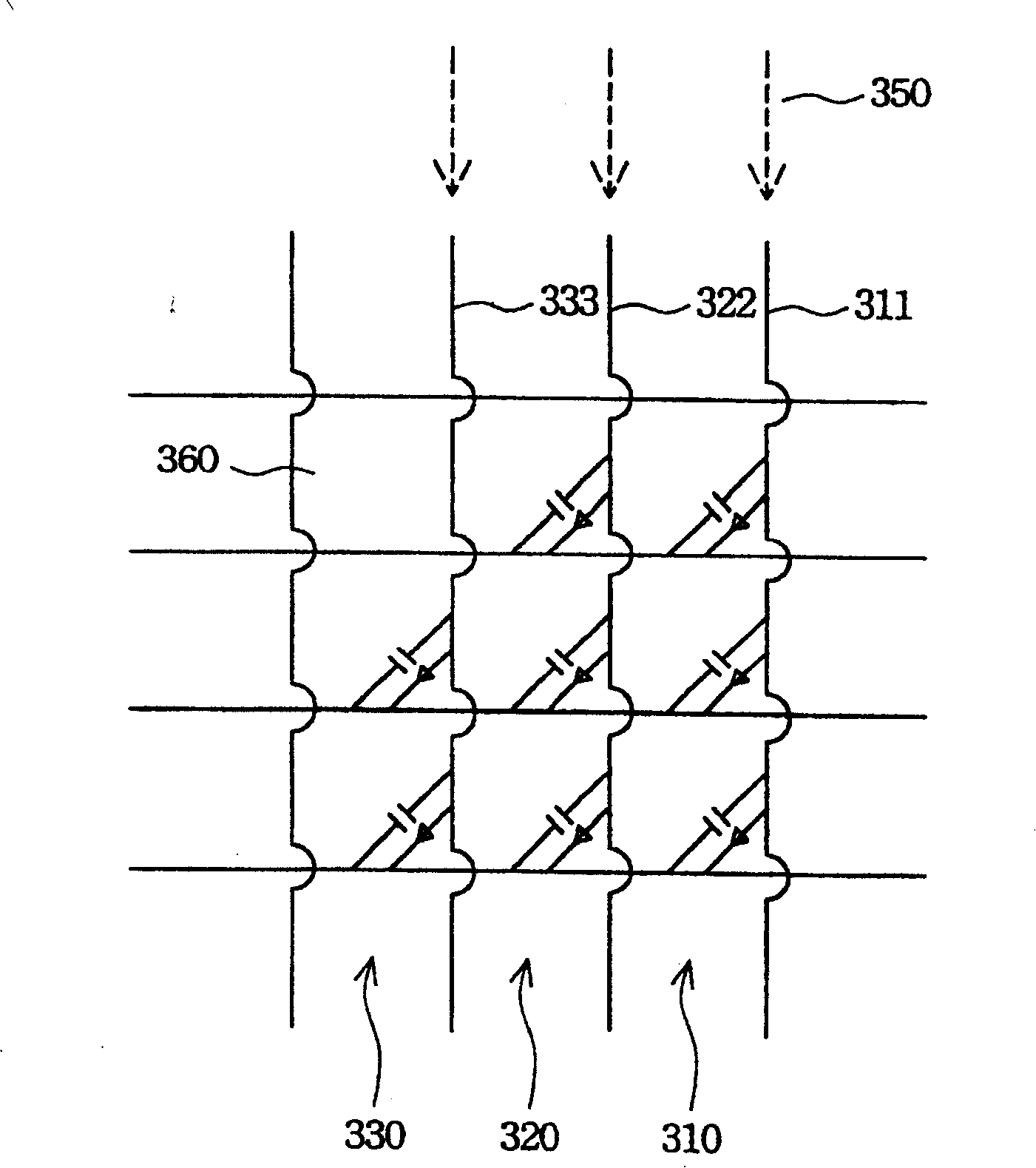
Therefore, for the main display area of ​​an organic light-emitting display panel, any display area where a line with a small capacitance value passes through will have a phenomenon of higher brightness, thus causing the defect of bright lines in the finished panel.

Method used


Image

  • Manufacturing method and structure of organic luminous display panel
  • Manufacturing method and structure of organic luminous display panel
  • Manufacturing method and structure of organic luminous display panel

Examples


Embodiment Construction

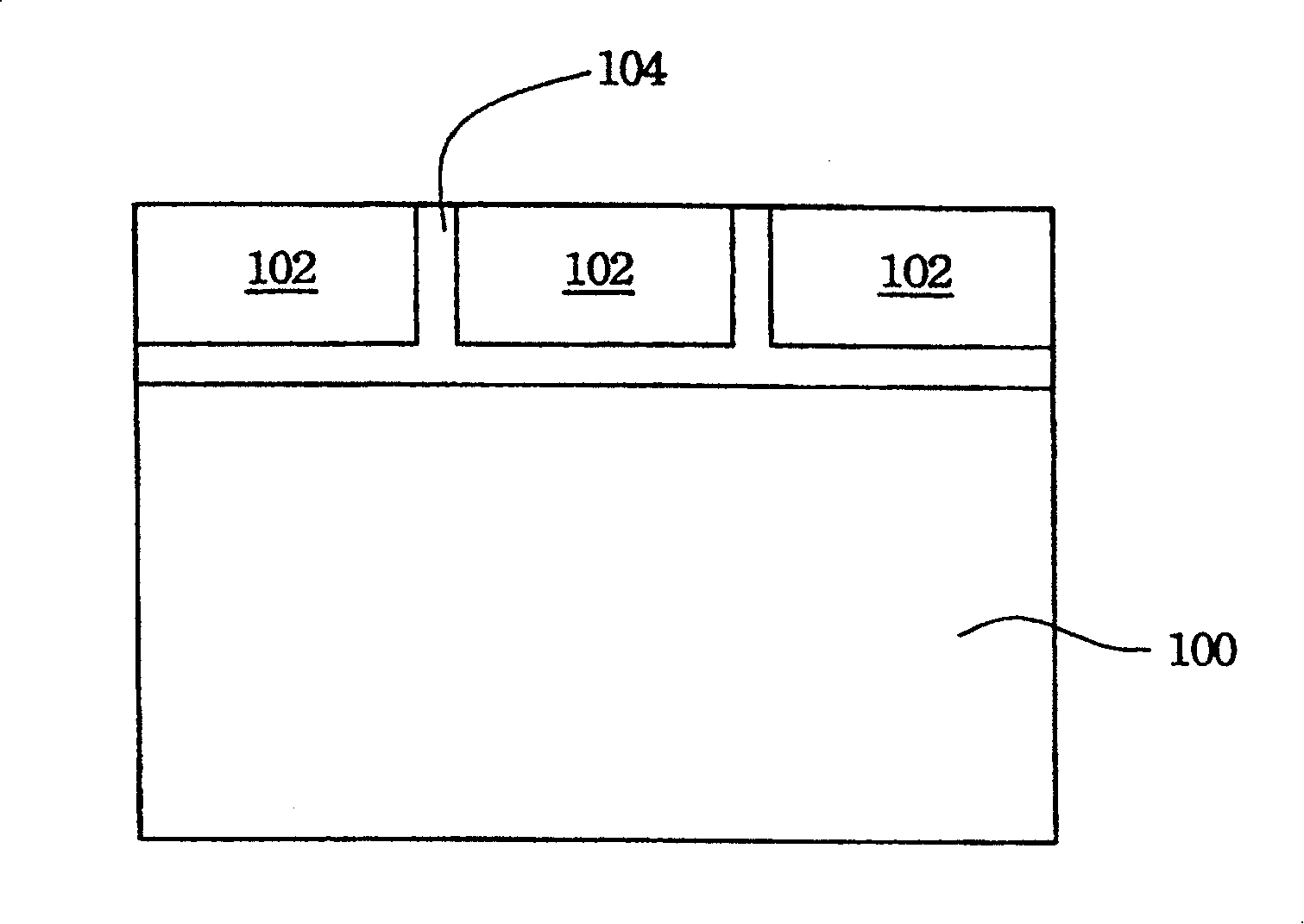
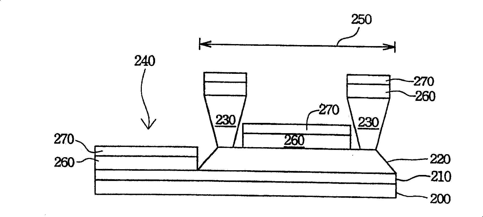
[0040] The invention is a manufacturing method and structure of an organic light-emitting display panel that can improve the bright line problem of the panel caused by the arrangement of non-luminous pixel areas around a specific image on the panel. By reducing the area occupied by the base layer, the area covered by the transparent electrode is reduced, so that part of the cathode conductive material on the non-luminous pixel area will not be completely isolated, but can provide part of the capacitance value when the current passes.

[0041] In this way, the originally low capacitance value of the lines passing through the non-luminous pixel area around the specific image is increased, so that the difference in the capacitance values ​​of the lines on the panel is reduced. As a result, the brightness distribution of the panel is more uniform, and the problem of bright lines is improved.

[0042] The method of the present invention will be described in detail below with a pref...


PUM


Abstract

A manufacturing method and structure of the organ light display panel. Use the figure set to reduce the covered area of the transparent electrode in the picture pels area without lighting on the panel, and make the anode and the cathode of the organ light diode respectively connect with the transparent electrode and metal electrode. It still partly has the property of the organ light diode. Change the picture pels area of born electro-property isolated without lighting into the picture area property that can provide the capacitance, when the data circuitry is charged. Therefore it makes the lighting situation of the panel homogeneous, and has efficiently improved the bright line objection of the panel.

Description

technical field [0001] The present invention relates to a method and a structure for manufacturing an organic light emitting display panel, in particular to a method and a structure for improving the bright line problem of the organic light emitting display panel. Background technique [0002] In recent years, in the flat panel display industry, organic light emitting displays (Organic Light Emitting Diode; OLED) have gradually attracted attention due to their advantages such as self-luminescence, high brightness, ultra-wide viewing angle, high response speed, low driving voltage, and light weight. . However, the current market share of organic light emitting displays is still limited. Therefore, major display manufacturers are trying to find the best manufacturing method to improve production yield and product characteristics, hoping to promote organic light emitting displays on the market as soon as possible. achieve popularization. [0003] In the existing organic light...

Claims


Application Information

Patent Timeline
Patent Type & Authority Patents(China)
IPC IPC(8): H01L51/56H01L51/50H05B33/10H05B33/12H05B33/14H05B33/26
Inventor 王赞纮丁定国张义林游丽莎
Owner TECO ELECTRIC AND MACHINERY
Learn More