
Method for improving bright line of splicing seam of display screen

A technology for splicing seams and display screens, which is applied to instruments, identification devices, etc., to improve the effect of bright lines and bright line problems.

Active Publication Date: 2020-05-19
KONKA GROUP
View PDF10 Cites 6 Cited by
  • Summary
  • Abstract
  • Description
  • Claims
  • Application Information

AI Technical Summary

Problems solved by technology

[0005] In view of the deficiencies in the prior art above, the purpose of the present invention is to provide a method for improving the bright line of the display screen splicing seam, aiming at improving the existing Micro-LED Or the problem of the bright line of the splicing seam on the Mini-LED display

Method used


Image

  • Method for improving bright line of splicing seam of display screen
  • Method for improving bright line of splicing seam of display screen
  • Method for improving bright line of splicing seam of display screen

Examples


Embodiment Construction

[0025] The present invention provides a method for improving the bright line of the splicing seam of a display screen. In order to make the purpose, technical solution and effect of the present invention clearer and clearer, the present invention will be further described in detail below with reference to the accompanying drawings and embodiments. It should be understood that the specific embodiments described here are only used to explain the present invention, and are not intended to limit the present invention.

[0026] The serial numbers assigned to components in this document, such as "first", "second", etc., are only used to distinguish the described objects, and do not have any sequence or technical meaning. In the present invention, "connection" and "connection" all include direct and indirect connection (connection) unless otherwise specified. In describing the present invention, it should be understood that the terms "upper", "lower", "front", "rear", "left", "right"...


PUM


Abstract

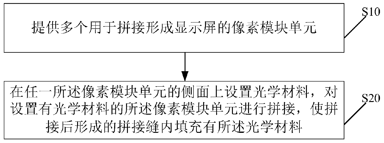
The invention discloses a method for improving a bright line of a splicing seam of a display screen, and the method comprises the steps: providing a plurality of pixel module units for splicing to form the display screen; arranging an optical material on the side face of any pixel module unit, splicing the pixel module units provided with the optical materia, and enabling a splicing seam formed after splicing to be filled with the optical material. Filling materials are arranged on the side faces of pixel module units used for being spliced to form the display screen, and splicing seams in thedisplay screen are filled with the filling materials after splicing. Due to the fact that the filling materials instead of air in the prior art are arranged between the splicing seams after splicing,total reflection cannot happen to the edges of the pixel module units easily, and the bright line problem of the splicing seams on the display screen is solved.

Description

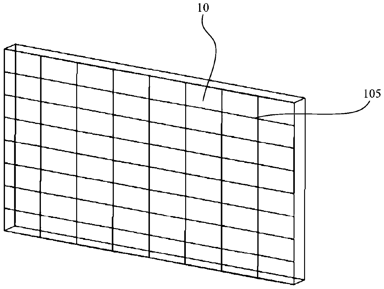
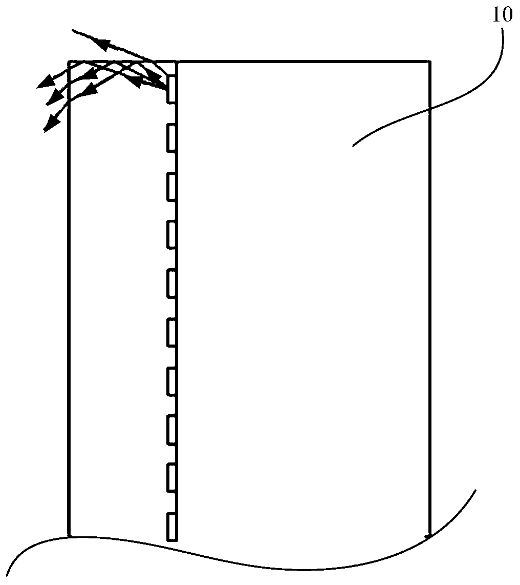
technical field [0001] The invention relates to the technical field of semiconductor photoelectric displays, in particular to a method for improving the bright line of a display screen splicing seam. Background technique [0002] Micro LED and Mini-LED are new display technologies, which have the same high color gamut and high contrast as OLED, but they are brighter than OLED, and have better reliability and lifespan. In the existing Micro LED and Mini-LED displays, each pixel is composed of three RGB chips, which are driven separately by RGB three primary color sub-pixels. Micro LED or Mini-LED displays are produced in modular assembly, such as figure 1 As shown, this can improve production efficiency; at the same time, it can improve the detection and repair efficiency of Micro LED and Mini-LED dead pixels. [0003] The light-emitting chip in the existing Micro-LED or Mini-LED display adopts epoxy resin or silicone protective layer. Since the refractive index of optical...

Claims


Application Information

Patent Timeline
Patent Type & Authority Applications(China)
IPC IPC(8): G09F9/302G09F9/33
CPCG09F9/302G09F9/3026G09F9/33
Inventor 钟文馗林伟瀚杨梅慧
Owner KONKA GROUP
Learn More