
Light-emitting device and method for manufacturing same

A technology for light-emitting devices and light-emitting surfaces, which is applied to lighting devices, semiconductor devices of light-emitting elements, light sources, etc., can solve problems such as inability to use, and achieve the effect of small difference in chromaticity characteristics and suppressing chromaticity deviation.

Inactive Publication Date: 2008-12-03
PANASONIC CORP
View PDF6 Cites 0 Cited by
  • Summary
  • Abstract
  • Description
  • Claims
  • Application Information

AI Technical Summary

Problems solved by technology

On the substrate 31 in this state, since a new semiconductor light emitting element 32 cannot be mounted again, the product becomes unusable.

Method used


Image

  • Light-emitting device and method for manufacturing same
  • Light-emitting device and method for manufacturing same
  • Light-emitting device and method for manufacturing same

Examples


Embodiment approach 1

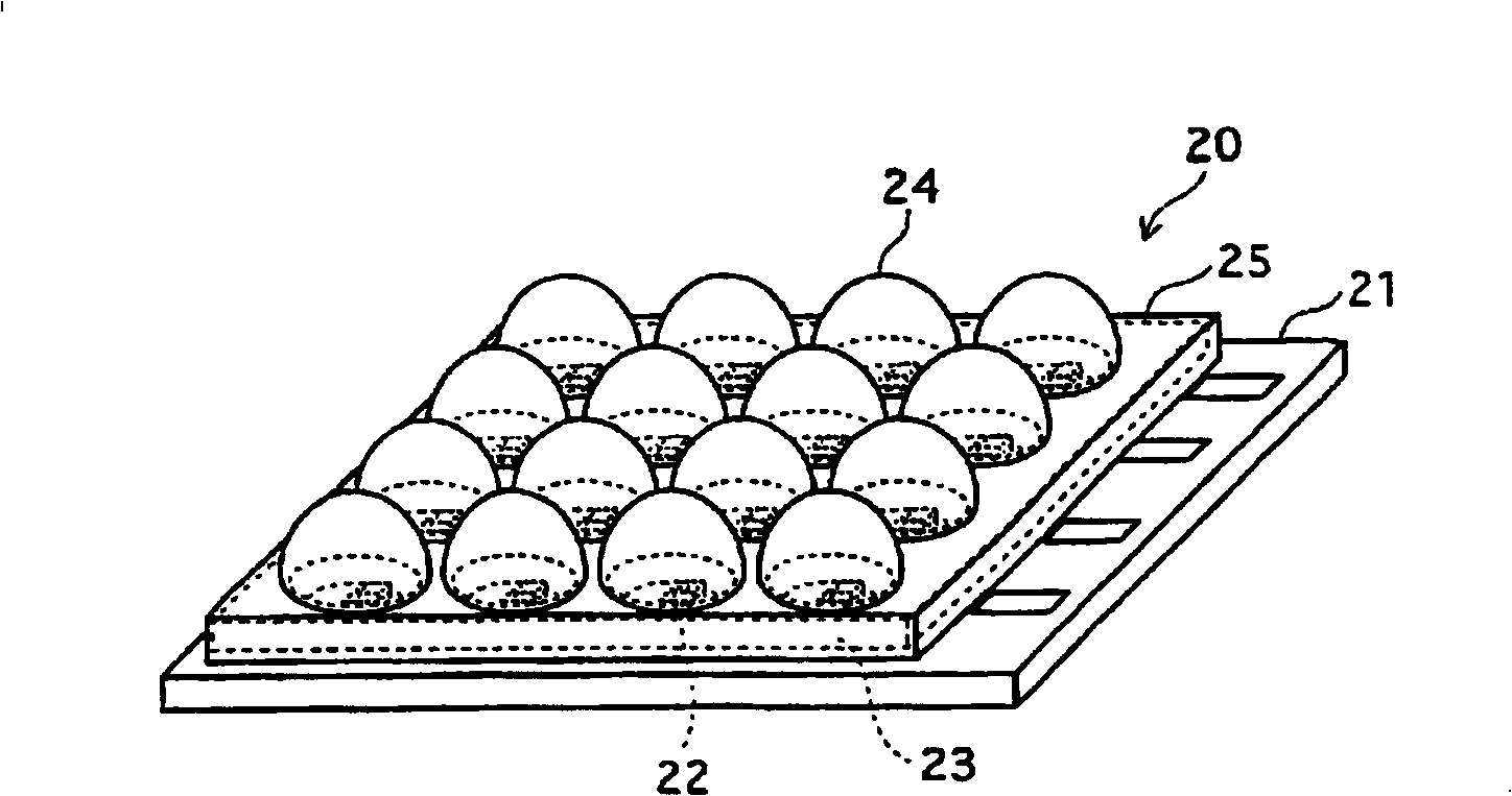
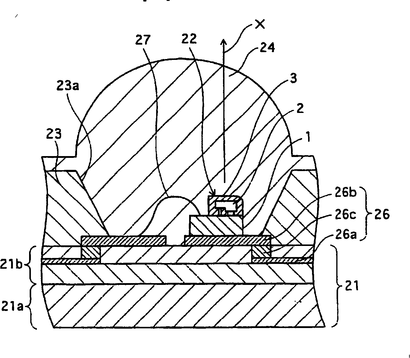
[0064] according to figure 2 and image 3 The configuration of a lighting device as a light emitting device according to Embodiment 1 of the present invention will be described. figure 2 It is a perspective view of the light emitting device according to Embodiment 1 of the present invention. image 3 is a partially enlarged cross-sectional view of the light emitting device.

[0065] Such as figure 2 and image 3 As shown, the lighting device 20 is composed of a substrate 21, a plurality of semiconductor components 22 mounted on the substrate 21, a reflective frame 23 with an opening at the position where the semiconductor component 22 is disposed on the substrate 21, and a reflective frame 23 formed to cover and The resin layer 25 which forms the convex lens part 24 in the light emitting direction of the semiconductor element 22 is comprised.

[0066] In addition, in the description of the lighting device according to Embodiment 1, the image 3 The light emitting dire...

Embodiment approach 2

[0115] according to Figure 14 The configuration of a lighting device as a light emitting device according to Embodiment 2 of the present invention will be described. Figure 14 It is a plan view of a light emitting device according to Embodiment 2 of the present invention.

[0116] The lighting device according to Embodiment 2 of the present invention is characterized in that figure 2 The configuration of the semiconductor component 22 of the lighting device shown is formed so that the positional relationship between the semiconductor light emitting element and the wire connection area of ​​the auxiliary mounting element loaded with the semiconductor light emitting element is different from that of other semiconductor components arranged adjacently in columns or rows. different.

[0117] again, in Figure 14 in, right with figure 2 The same symbols are assigned to the same structures, and explanations are omitted.

[0118] Such as Figure 14 As shown, the lighting dev...


PUM


Abstract

In a light emitting apparatus that includes a plurality of semiconductor light emitting devices 2 each having a light emitting face covered with a phosphor layer 3, a semiconductor assembly obtained by assembling a submount and the semiconductor light emitting devices is mounted on the substrate. Accordingly, chromaticity characteristics of the semiconductor assembly can be measured before the semiconductor assembly is mounted on the substrate. Therefore, even if using a plurality of semiconductor light emitting devices, a semiconductor assembly can be prepared on which the semiconductor light emitting devices each having uniform chromaticity characteristics are mounted before the semiconductor assembly is mounted on the substrate. And, a light emitting apparatus having suppressed dispersion of chromaticity can be manufactured.

Description

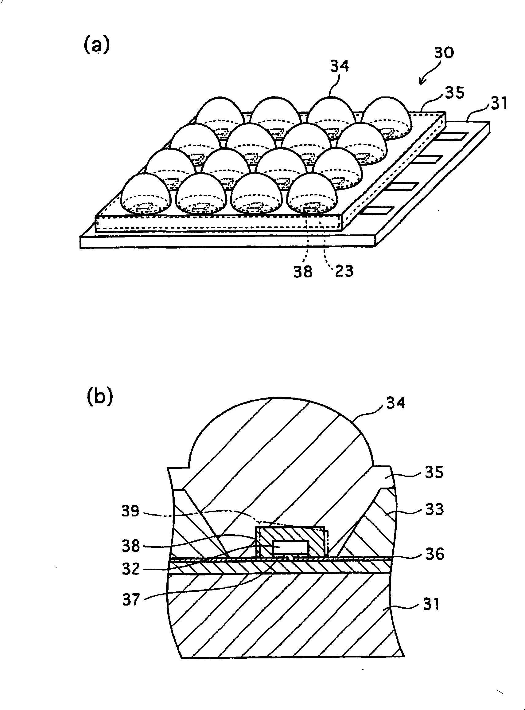
technical field [0001] The present invention relates to a light-emitting device including a plurality of semiconductor light-emitting elements and a substrate covering at least a part of a light-emitting surface with a phosphor layer, and a method of manufacturing the same. Background technique [0002] A conventional light-emitting device is a device in which a plurality of semiconductor light-emitting elements are mounted on a substrate, and the semiconductor light-emitting elements are covered with a resin containing a fluorescent substance. As such a conventional light emitting device, a light emitting device described in Patent Document 1 is known. [0003] according to figure 1 The structure of a conventional light-emitting device will be described. figure 1 is an existing lighting device, figure 1 (a) is an oblique view, figure 1 (b) is a partially enlarged cross-sectional view. [0004] Such as figure 1 As shown in (a) and (b), the existing light-emitting devic...

Claims


Application Information

Patent Timeline
Patent Type & Authority Patents(China)
IPC IPC(8): H01L33/00F21K99/00H01L25/075H01L25/16H01L33/50
CPCH01L33/505H01L25/0753H01L2224/16145H01L2924/10253F21K9/00H01L2933/0025H01L2224/48091H01L2224/05573H01L2224/05568H01L2924/00014H01L24/16H01L2224/06102H01L2224/1703H01L2924/00H01L2224/05599
Inventor 小原邦彦前田俊秀矢野正谷本宪保
Owner PANASONIC CORP
Learn More