Electronic device with fan-out block possessing homogeneous impedance

An electronic device and impedance value technology, which is applied in the field of thin film transistor liquid crystal display panels, can solve the problems of impedance value difference, adjacent impedance value difference, etc.

Active Publication Date: 2009-10-21
AU OPTRONICS CORP
View PDF6 Cites 0 Cited by
  • Summary
  • Abstract
  • Description
  • Claims
  • Application Information

AI Technical Summary

Problems solved by technology

For the impedance value difference between each fan-out block, none of the above-mentioned patent documents mentions it; moreover, if the method disclosed in the above-mentioned patent document is used, the adjacent impedance of the junction 5 of adjacent fan-out blocks values ​​will have differences, still doesn't solve the problem

Method used


Image

  • Electronic device with fan-out block possessing homogeneous impedance
  • Electronic device with fan-out block possessing homogeneous impedance
  • Electronic device with fan-out block possessing homogeneous impedance

Examples


Embodiment Construction

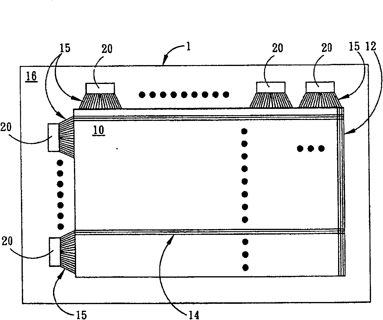
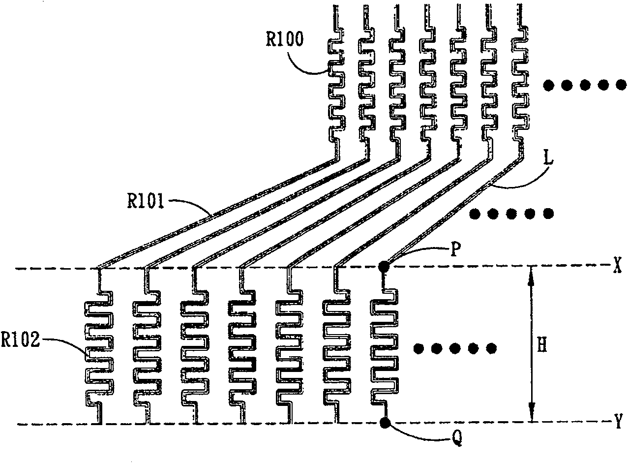
[0041] In the liquid crystal display panel disclosed in the embodiment of the present invention, except for the fan-out block, the other figure 1 The shown structures are the same, so the figure is used here, and the description of each component is omitted. image 3 The internal structure of the fan-out block of the embodiment of the present invention is shown, which includes a plurality of connecting wires L, and each connecting wire L includes at least three regions, which are respectively: the first routing connection region R100, which is connected to the bonding region 20( figure 1 ) bonding pads, thus electrically connected to the driver integrated circuit; the second winding connection region R102, which is connected to the data line 12 or the gate line 14; and the relay connection region R101, which is located between the first winding connection region R100 and between the second winding connection regions R102. In this example, the first wire connection region R10...


PUM


Abstract

The present invention proposes an electronic device and a production method thereof, wherein the intercepts of the connection areas on the side of the active area of ​​the outer connection wires of adjacent fan-out blocks are different from each other. In this way, the outer wires at the intersection of adjacent fan-out blocks have approximately equal resistance values; thus, the overall wires across adjacent fan-out blocks have uniform resistance values, so as to ensure the operation quality of the electronic device.

Description

technical field [0001] The present invention relates to an electronic device with uniform impedance fan-out blocks, in particular to a thin film transistor liquid crystal display panel with uniform impedance fan-out blocks (thin film transistor LCD panel or TFT LCD panel). Background technique [0002] figure 1 The lower substrate 1 of a general active matrix thin film transistor liquid crystal display panel mainly includes an active area 10 . The active area 10 has data lines 12 and gate lines 14 for controlling transistor switches (not shown in the figure) to display images in each pixel. In this specification, the data lines 12 and the gate lines 14 are also collectively referred to as control lines. The peripheral portion of the active region 10 is called an outer-lead bonding area (OLB area) 16, on which a plurality of bonding areas (bonding areas) 20 are arranged; each bonding area 20 has some bonding pads (bonding pads), used to join the driver integrated circuit ...

Claims


Application Information

Patent Timeline
Patent Type & Authority Patents(China)
IPC IPC(8): G02F1/136G02F1/133G02F1/1345H01L27/12H01L23/52
Inventor 李敏勤赖明升
Owner AU OPTRONICS CORP
Why Eureka
Try Eureka