Supercharge Your Innovation With Domain-Expert AI Agents!

TFT, method of manufacturing the TFT, flat panel display having the TFT, and method of manufacturing the flat panel display

一种平板显示器、制造方法的技术,应用在半导体/固态器件制造、电固体器件、半导体器件等方向,能够解决有机半导体破坏等问题

Active Publication Date: 2009-12-02
SAMSUNG DISPLAY CO LTD
View PDF4 Cites 0 Cited by
  • Summary
  • Abstract
  • Description
  • Claims
  • Application Information

AI Technical Summary

Problems solved by technology

[0010] However, organic semiconductor films cannot be patterned by conventional patterning methods known as photolithography
Patterning methods can be used to make active trenches, but it usually involves wet or dry etching, thus causing damage to the organic semiconductor

Method used


Image

  • TFT, method of manufacturing the TFT, flat panel display having the TFT, and method of manufacturing the flat panel display
  • TFT, method of manufacturing the TFT, flat panel display having the TFT, and method of manufacturing the flat panel display
  • TFT, method of manufacturing the TFT, flat panel display having the TFT, and method of manufacturing the flat panel display

Examples


Embodiment Construction

[0025] Hereinafter, exemplary embodiments of the present invention will be described by referring to the accompanying drawings.

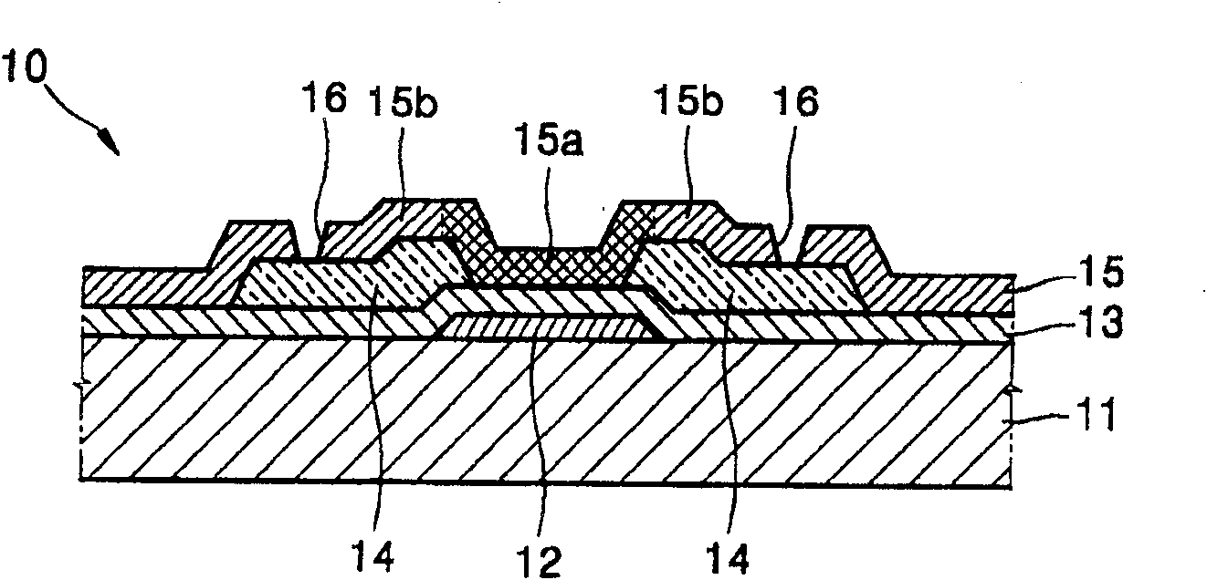
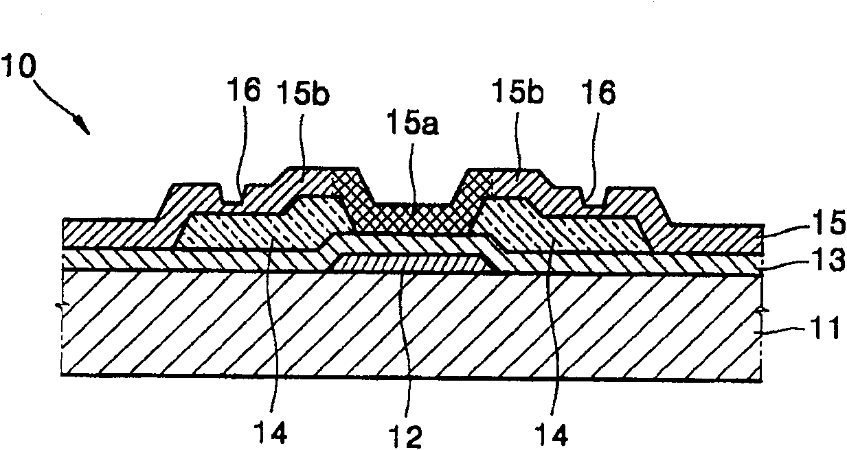
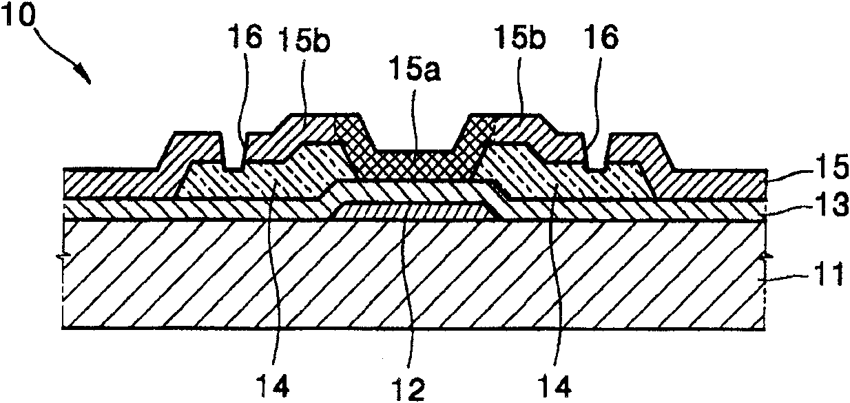
[0026] figure 1 is a cross-sectional view of a TFT 10 according to an exemplary embodiment of the present invention.

[0027] refer to figure 1 , the TFT 10 may be formed on a substrate 11, and the substrate 11 may be formed of glass or plastic.

[0028] The gate electrode 12 is formed in a pre-pattern on the substrate 11 , and the gate insulating film 13 covers the gate electrode 12 . Source and drain electrodes 14 are formed on the gate insulating film 13, respectively. Although they can be used with figure 1 The gates 12 are shown partially overlapping, but the invention is not limited thereto. A semiconductor film 15 is formed on the source and drain electrodes 14 .

[0029] The semiconductor film 15 includes source and drain regions 15b and a channel region 15a connecting the source and drain regions 15b. The source and drain regions 15b...


PUM


Abstract

A thin film transistor (TFT) including a semiconductor film that may be simply patterned, a method of manufacturing the TFT, a flat panel display (FPD) including the TFT, and a method of manufacturing the FPD. The TFT includes a gate electrode, source and drain electrodes electrically insulated from the gate electrode, and a semiconductor film electrically insulated from the gate electrode and including source and drain regions coupled to the source and drain electrodes, respectively, and a channel region coupling the source and drain regions. The semiconductor film has a groove that isolates the channel region from an adjacent TFT.

Description

[0001] This application claims priority from Korean Patent Application No. 10-2004-0036635 filed May 22, 2004, which is hereby incorporated by reference in its entirety. technical field [0002] The present invention relates to a thin film transistor (TFT), a method of manufacturing the TFT, a flat panel display (FPD) including the TFT and a method of manufacturing the FPD. More specifically, the present invention relates to a TFT including a semiconductor film that can be easily patterned, a method of manufacturing the TFT, an FPD including the TFT, and a method of manufacturing the FPD. Background technique [0003] Generally, TFTs can be used in FPDs such as liquid crystal displays (LCDs), organic electroluminescence (EL) displays, and inorganic EL displays as switching devices that turn on and off pixels and driving devices that drive pixels. [0004] A TFT generally includes a semiconductor film, a gate, and source and drain electrodes. The semiconductor film may inclu...

Claims


Application Information

Patent Timeline
Patent Type & Authority Patents(China)
IPC IPC(8): H01L29/786H01L27/12H01L21/336H01L21/84H01L51/05H01L21/304H01L21/762H01L21/77H01L51/40
CPCH01L27/1248H01L27/1222H01L29/78681H01L29/78606H01L29/66742H01L21/76264H01L27/12H01L27/1214H01L29/78696H10K10/484
Inventor 徐旼彻杨南喆具在本姜泰旻金慧东
Owner SAMSUNG DISPLAY CO LTD
Features
  • R&D
  • Intellectual Property
  • Life Sciences
  • Materials
  • Tech Scout
  • Unparalleled Data Quality
  • Higher Quality Content
  • 60% Fewer Hallucinations
Learn More