Supercharge Your Innovation With Domain-Expert AI Agents!

Image sensor fabricating method

A technology of image sensor and manufacturing method, which is applied in semiconductor/solid-state device manufacturing, electric solid-state devices, semiconductor devices, etc., and can solve problems such as difficult standardization of focal lengths, great changes in focal lengths, difficult standardization of focal lengths of microlenses, etc.

Inactive Publication Date: 2010-02-24
DONGBU HITEK CO LTD
View PDF3 Cites 0 Cited by
  • Summary
  • Abstract
  • Description
  • Claims
  • Application Information

AI Technical Summary

Problems solved by technology

[0004] Also, the focal length of the microlenses can vary widely
In addition, it is difficult to standardize the focal length of the microlens
That is, since a basic pattern is formed on a lens-forming photosensitive layer by defocusing of a scanner, and microlenses are generally manufactured by performing a thermal reflow process on such a photosensitive layer, the focal length may vary greatly, and Focal length is difficult to standardize
Thus, replicating the microlens shape within certain manufacturing tolerances can be challenging

Method used


Image

  • Image sensor fabricating method
  • Image sensor fabricating method
  • Image sensor fabricating method

Examples


Embodiment Construction

[0009] In describing the following embodiments, it will be understood that when a layer (or film) is referred to as being "on / over" another layer or substrate, that layer (or film) can be directly on the other layer or substrate. on the substrate, or an intervening layer may also be present. Further, it will be understood that when a layer is referred to as being 'under' another layer, it can be directly under the other layer, or one or more intervening layers may also be present. In addition, it will also be understood that when a layer is referred to as being "between" two layers, it can be the only layer between the two layers, or one or more intervening layers may also be present.

[0010] Reference will now be made in detail to embodiments of the invention, examples of which are illustrated in the accompanying drawings.

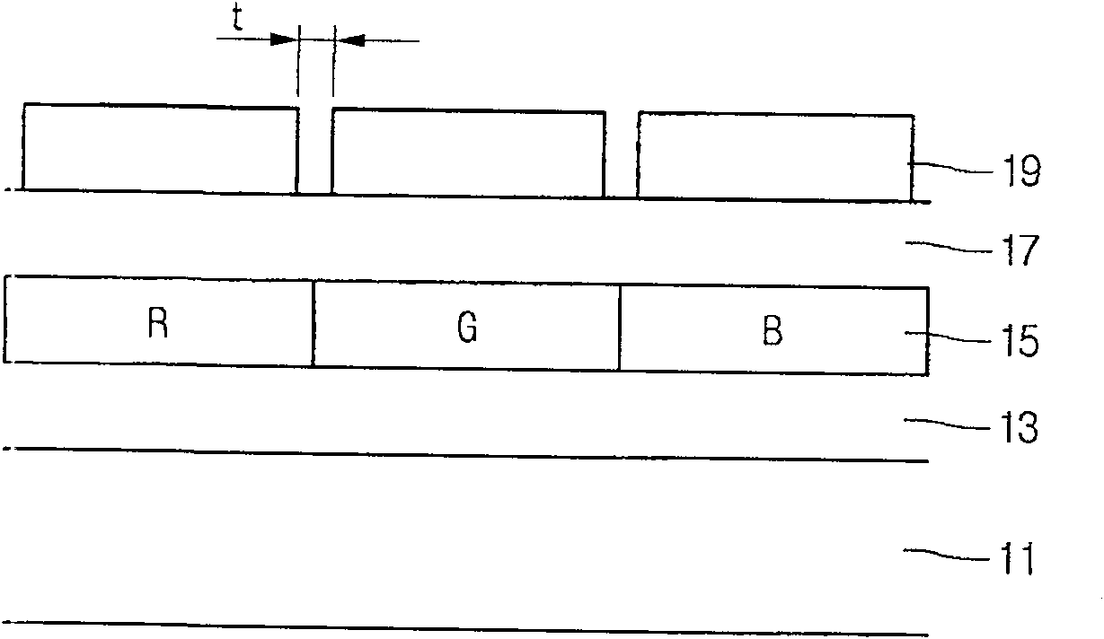
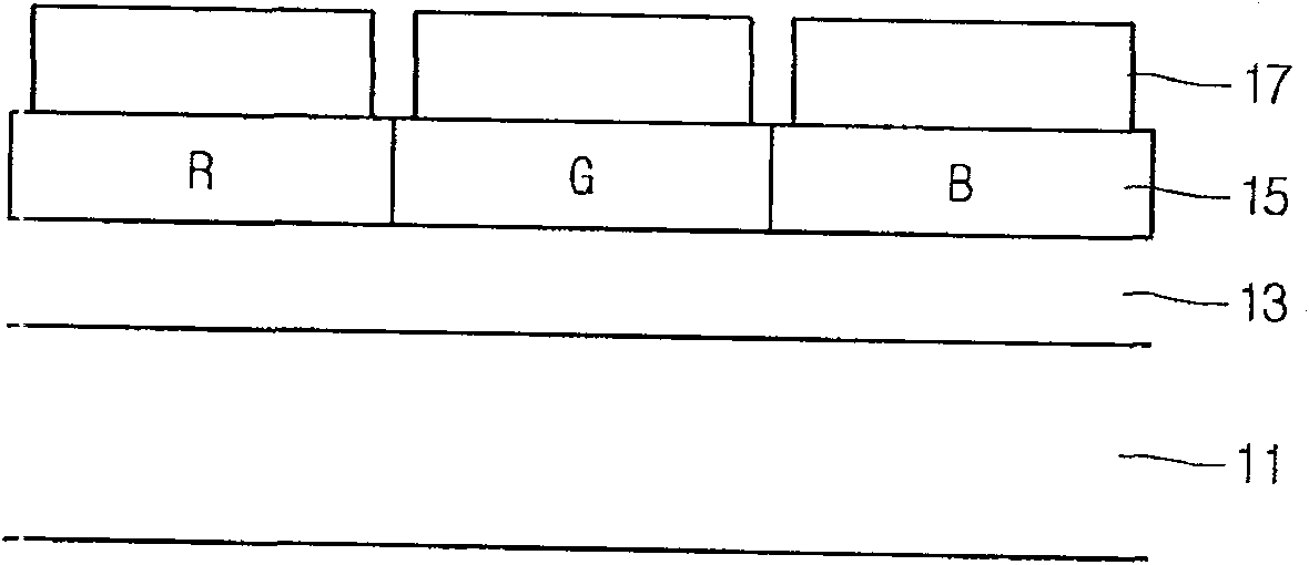
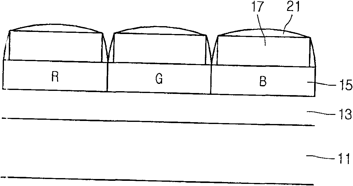
[0011] Figure 1-Figure 4 It is a schematic diagram conceptually illustrating a manufacturing method of an image sensor according to an embodiment of t...


PUM


Abstract

A method of fabricating an image sensor includes forming a first SiO2 layer on a color filter layer, patterning a photosensitive layer on first SiO2 layer, patterning the first SiO2 layer through a first etching process, forming a second SiO2 layer on the first SiO2 layer, and forming a micro-lens by etching the second SiO2 layer.

Description

technical field [0001] Embodiments of the present invention relate to an image sensor and a method of manufacturing the same. Background technique [0002] Generally, in a complementary metal oxide semiconductor (CMOS) image sensor, microlenses are formed on the uppermost layer. The light gathered by the microlens passes through the color filter array layer and the planarization layer, and is converted into an electrical signal by a light receiving unit such as a photodiode. [0003] The image sensor displays an image using the converted electrical signal. Here, the focal length of the microlens, the size and distribution of the color filters, the thickness of the planarization layer, and the pitch of the photodiodes should be determined on the basis of considering the correlation among them. [0004] At the same time, the focal length of the microlenses may vary widely. Furthermore, it is difficult to standardize the focal length of the microlenses. That is, since a bas...

Claims


Application Information

Patent Timeline
Patent Type & Authority Patents(China)
IPC IPC(8): H01L21/82H01L21/71H01L27/146
CPCH01L27/14685H01L27/14627H01L27/146
Inventor 赵殷相
Owner DONGBU HITEK CO LTD
Features
  • R&D
  • Intellectual Property
  • Life Sciences
  • Materials
  • Tech Scout
  • Unparalleled Data Quality
  • Higher Quality Content
  • 60% Fewer Hallucinations
Learn More