Forming Substrate Structure by Filling Recesses with Deposition Material

a technology of deposition material and substrate, which is applied in the direction of basic electric elements, semiconductor/solid-state device manufacturing, electric apparatus, etc., can solve the problems of reducing affecting the reliability of semiconductor devices, and affecting the stability of substrates

Inactive Publication Date: 2010-02-18
VEECO ALD
View PDF11 Cites 387 Cited by
  • Summary
  • Abstract
  • Description
  • Claims
  • Application Information

AI Technical Summary

Problems solved by technology

These conventional techniques, however, are not suitable to fill the trenches in cases where 45 nm or smaller design rules apply, or an aspect ratio of 5:1 or larger applies.
Consequently, voids 4 are formed in the recess, which reduces the reliability of the semiconductor device.
Hence, this convention technique may cause damage to the substrate 1 by bias or plasma.
Further, if the aspect ratio of the recess 2 is high, then the recess 2 may be filled partially, resulting in uneven coating of the substrate 1.

Method used


Image

  • Forming Substrate Structure by Filling Recesses with Deposition Material
  • Forming Substrate Structure by Filling Recesses with Deposition Material
  • Forming Substrate Structure by Filling Recesses with Deposition Material

Examples


Embodiment Construction

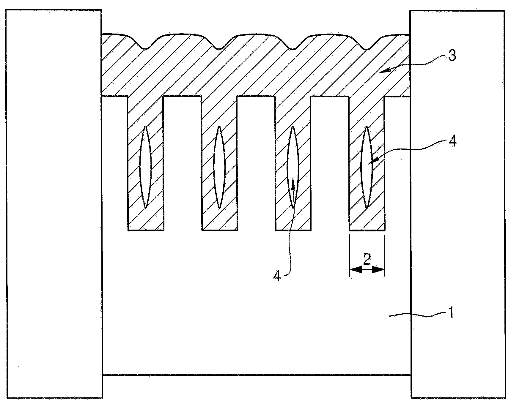
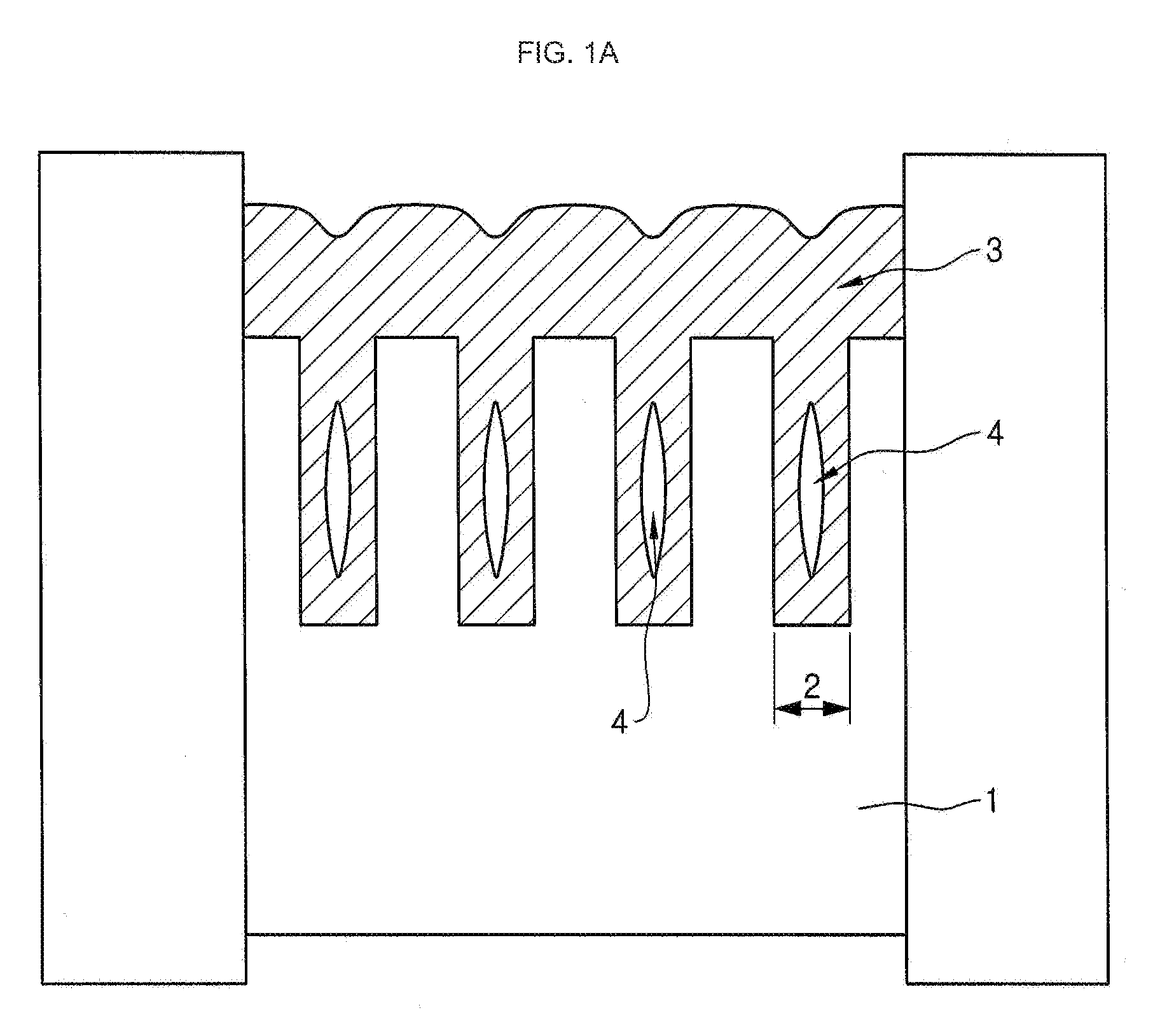
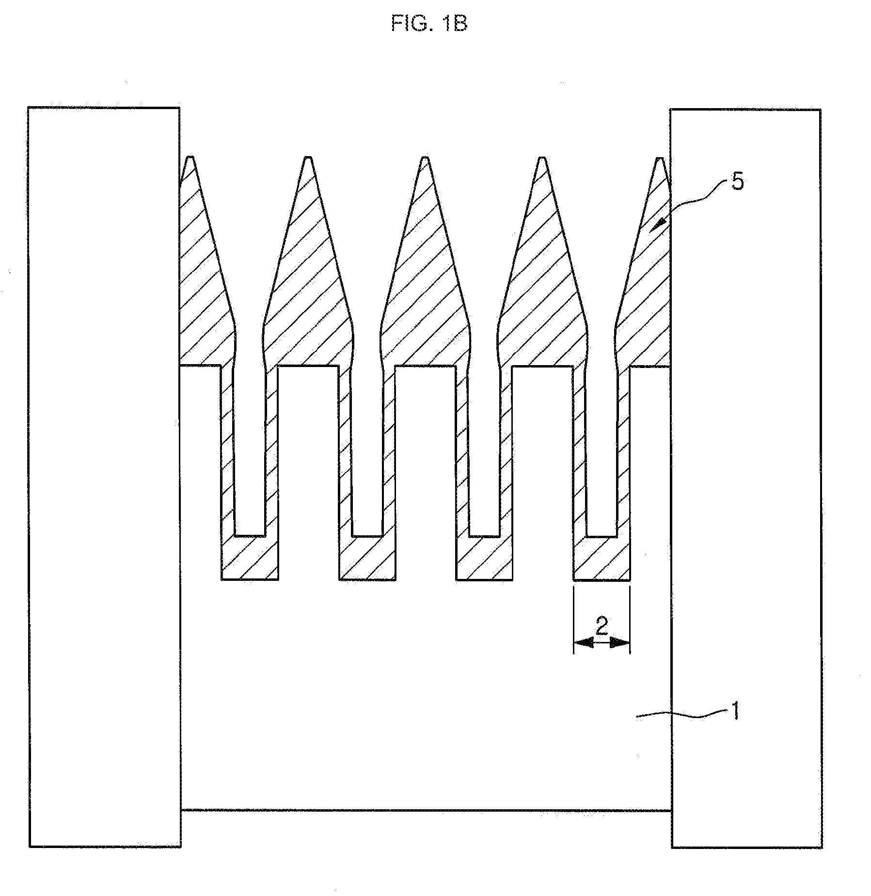
[0018]Hereinafter, reference will now be made in detail to various example embodiments, examples of which are illustrated in the accompanying drawings and described below. While the invention will be described in conjunction with example embodiments, it will be understood that the present description is not intended to limit the invention to those example embodiments. On the contrary, the invention is intended to cover not only the example embodiments, but also various alternatives, modifications, equivalents and other embodiments, which may be included within the spirit and scope of the invention as defined in the appended claims. In the following, description of known functions or constructions which may unnecessarily obscure the subject matter of the present invention will be omitted.

[0019]The number and types of atoms or molecules constituting each material are provided in Figures for the purpose of illustration. The present invention is not limited by the number and types of at...


PUM

PropertyMeasurementUnit
aspect ratioaaaaaaaaaa
structureaaaaaaaaaa
dielectricaaaaaaaaaa

Abstract

A substrate structure is produced by forming a first material layer on a substrate having a recess, removing the first material layer from the portion of the substrate except for the recess using a second material that reacts with the first material, and forming a deposition film from the first material layer using a third material that reacts with the first material. A method of manufacturing a device may include the method of forming a substrate structure.

Description

CROSS-REFERENCE TO RELATED APPLICATION[0001]This application claims priority under 35 U.S.C. §119(e) to co-pending U.S. Provisional Patent Application No. 61 / 088,679 entitled “Method of Forming Substrate Structure and Method of Manufacturing Device Comprising the Same” filed on Aug. 13, 2008, which is incorporated by reference herein in its entirety.BACKGROUND[0002]1. Field of Art[0003]This invention relates to forming a substrate structure with deposition material filling one or more recesses on a substrate.[0004]2. Description of Related Art[0005]Many semiconductor devices include transistors, wirings, insulators and other components formed on a substrate. Conventionally, transistors are insulated from each other using technique such as LOCOS (local oxidation of silicon) or SEPOX (selective poly oxidation). To accommodate semiconductor devices with smaller components for higher level of integration, a technique called STI (Shallow Trench Isolation) was developed. The STI forms tre...

Claims


Application Information

Patent Timeline
Patent Type & Authority Applications(United States)
IPC IPC(8): H01L21/20H01L21/31H01L21/3205
CPCH01L21/02274H01L21/02277H01L21/0228H01L21/02315H01L21/76224H01L21/02554H01L21/0262H01L21/3141H01L21/31604H01L21/0254
Inventor LEE, SANG IN
Owner VEECO ALD
Why Eureka
Try Eureka