Method for fabricating semiconductor device

a semiconductor device and fabrication method technology, applied in semiconductor devices, semiconductor/solid-state device details, electrical devices, etc., can solve the problems of mechanically weaker film strength, inter-wire parasitic capacity and signal transmission delay due to wire resistance, and the damage of sico film by coating method or cvd process,

Inactive Publication Date: 2010-11-30
KK TOSHIBA
View PDF8 Cites 397 Cited by
  • Summary
  • Abstract
  • Description
  • Claims
  • Application Information

AI Technical Summary

Benefits of technology

[0011]A method for fabricating a semiconductor device according to another aspect of the present invention includes forming a porous dielectric film above a substrate using a porous insulating material, exposing the porous dielectric film to an oxygen plasma atmosphere, and repairing film quality of the porous dielectric film by feeding a predetermined material that replaces a Si—OH group and also has a Si—C—Si bond to the porous dielectric film exposed to the oxygen plasma atmosphere.

Problems solved by technology

However, as semiconductor devices become still finer, problems of a so-called inter-wire parasitic capacity and a signal transmission delay due to wire resistance have arisen.
However, such dielectric films having lower dielectric constants pose, on the other hand, a problem of mechanically weaker film strength.
Here, a SiCO film by the coating method or CVD process is known to be damaged by etching when forming a via hole or trench or in processes such as plasma ashing for separating a mask for etching and cleaning by a chemical solution.
Thus, there has been a problem of increased hygroscopicity of the film.
Therefore, the film will be damaged in a wider range.
Further, the inclusion of moisture increases the dielectric constant and also oxidizes metal wires in post process, particularly in a thermal operation, causing a failure leading to degradation of wiring reliability.
In such a case, a failure phenomenon of diffusion of Cu from a Cu wiring portion into the low-k film will be caused in post process or when a semiconductor device is operating.
Such a failure phenomenon will lead to a problem of causing an open failure of metal wiring in the end.
However, pores exposed on the low-k film surface cannot be closed by these repair technologies.
Moreover, with these repair technologies, mechanical strength of the low-k film is not sufficient.

Method used


Image

  • Method for fabricating semiconductor device
  • Method for fabricating semiconductor device
  • Method for fabricating semiconductor device

Examples


first embodiment

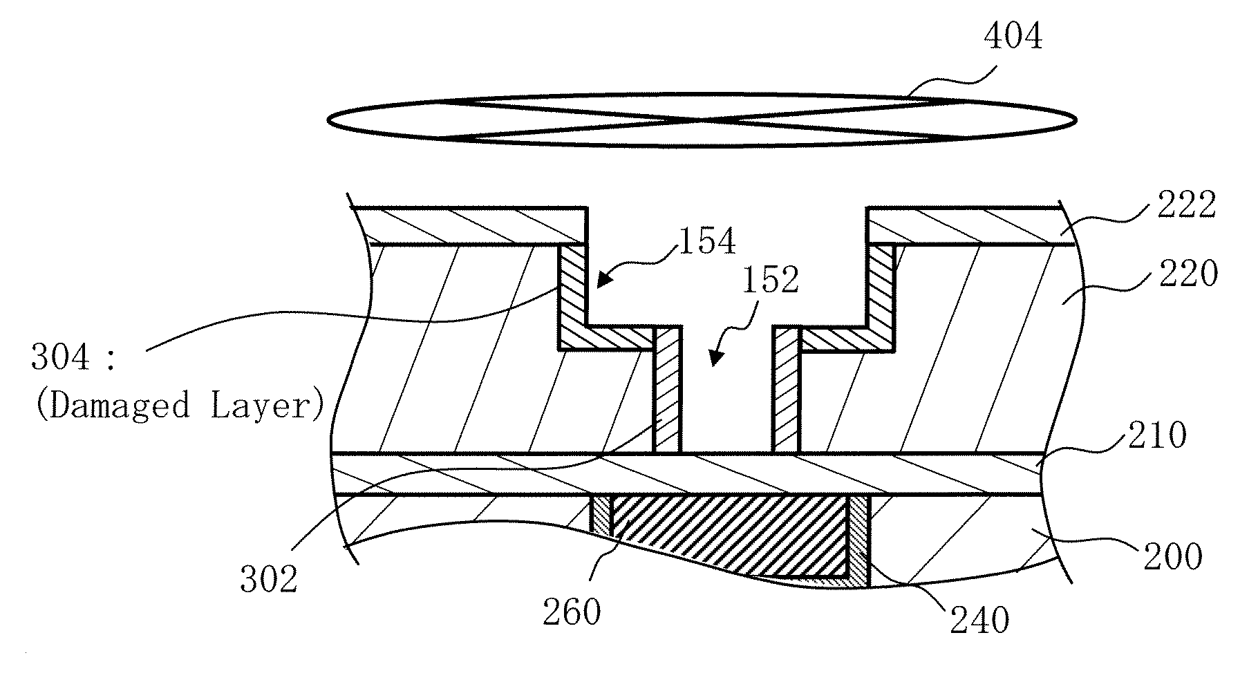
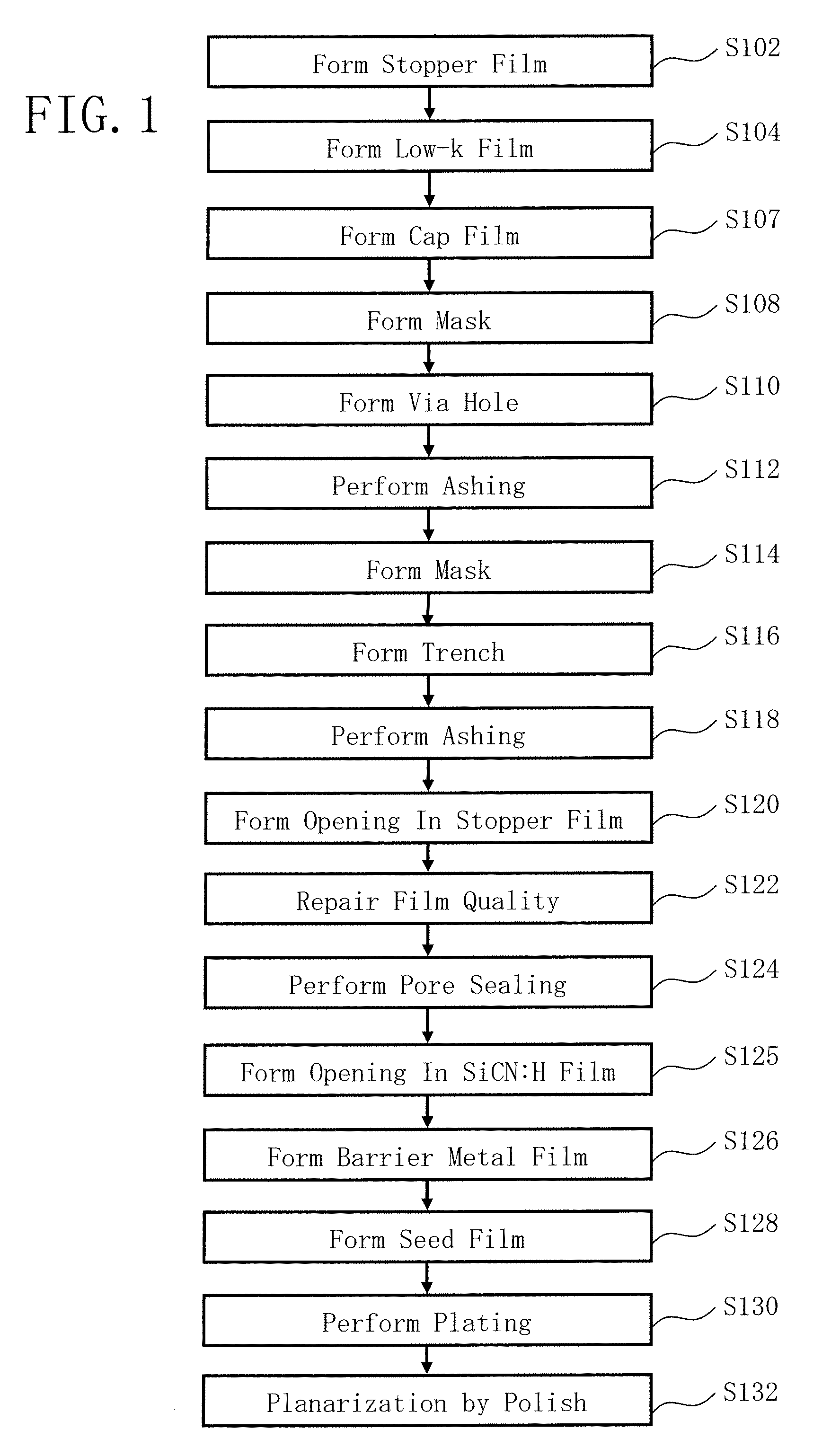
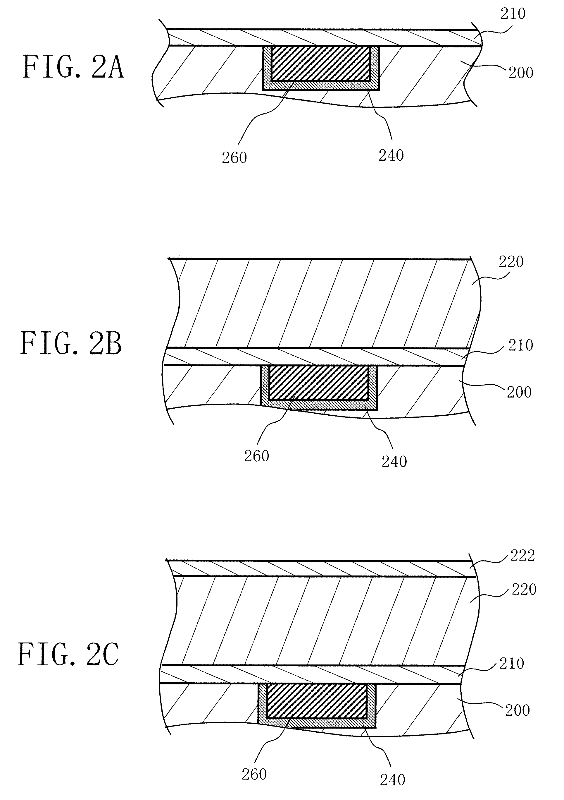
[0034]A first embodiment will be described below using drawings. FIG. 1 is a flow chart showing principal parts of a method for fabricating a semiconductor device in the first embodiment. In FIG. 1, the present embodiment performs a series of processes including a stopper film formation process (S102) to form a stopper film, a low-k film formation process (S104) to form a low dielectric constant insulating material (low-k material) film, a cap film formation process (S107) to form a cap film, a mask formation process (S108) to form a mask, a via hole formation process (S110) to form a via hole, an ashing process (S112), a mask formation process (S114) to form a mask, a trench formation process (S116) to form a trench, an ashing process (S118), a stopper film opening process (S120), a film quality repair process (S122) to repair film quality, a pore sealing process (S124), a SiCN:H film opening process (S125), a barrier metal film formation process (S126), a seed film formation proce...

second embodiment

[0072]In the first embodiment, the manufacturing method for a semiconductor device was described by focusing on repairs of a damaged layer and pore sealing. In a second embodiment, a manufacturing method for a semiconductor device will be described by focusing on repairs of a damaged layer, improvement of mechanical strength, and improvement of plasma resistance.

[0073]FIG. 11 is a flow chart showing principal parts of a method for fabricating a semiconductor device in the second embodiment. In FIG. 11, the second embodiment performs a series of processes including the stopper film formation process (S102) to form a stopper film, the low-k film formation process (S104) to form a low dielectric constant insulating material (low-k material) film, the cap film formation process (S107) to form a cap film, the mask formation process (S108) to form a mask, the via hole formation process (S110) to form a via hole, the ashing process (S112), a film quality repair process (S113) to repair fil...

third embodiment

[0098]Material in the form of gas that can be used for the repair reaction and incorporation of Si—C—Si backbone structures into the film in the second embodiment may be used as a gas used for the film quality repair process and the pore sealing process in the first embodiment. That is, a gas having a Si—R1 group replacing the Si—OH group and also the Si—C—Si bond is used. Accordingly, in addition to effects of the first embodiment, mechanical strength and plasma resistance of the low-k film 220 can further be improved. Gases of materials that can be used in the second embodiment for film quality repairs react very rarely and a reaction with each other seldom occurs. For example, Si(CH3)2NH2SiCH2Si(CH3)2NH2 reacts with each other very rarely during film quality repairs and a reaction with each other seldom occurs. Then, a pore sealing film can be formed in the pore sealing process by making the gas react with each other by providing reaction energy of plasma or the like. Thus, with ...


PUM

PropertyMeasurementUnit
thicknessaaaaaaaaaa
relative dielectric constantaaaaaaaaaa

Abstract

A method for fabricating a semiconductor device, includes forming a porous dielectric film above a substrate using a porous insulating material, forming an opening in the porous dielectric film, repairing film quality of the porous dielectric film on a surface of the opening by feeding a predetermined gas replacing a Si—OH group to the opening, and performing pore sealing of the surface of the opening using the same predetermined gas as that used for film quality repairs after repairing the film quality.

Description

CROSS-REFERENCE TO RELATED APPLICATION[0001]This application is based upon and claims the benefit of priority from prior Japanese Patent Application No. 2006-299022 filed on Nov. 2, 2006 in Japan, the entire contents of which are incorporated herein by reference.BACKGROUND OF THE INVENTION[0002]1. Field of the Invention[0003]The present invention relates to a method for fabricating a semiconductor device, and for example, relates to a method for fabricating a semiconductor device forming a porous low dielectric constant dielectric film.[0004]2. Related Art[0005]With increasingly more microscopic and faster semiconductor devices, a wiring structure is moving from a single layer to multiple layers and semiconductor devices having five layers or more of metallic wiring structures have been developed and manufactured. However, as semiconductor devices become still finer, problems of a so-called inter-wire parasitic capacity and a signal transmission delay due to wire resistance have ari...

Claims


Application Information

Patent Timeline
Patent Type & Authority Patents(United States)
IPC IPC(8): H01L21/00
CPCH01L21/02126H01L21/02203H01L21/02216H01L21/02282H01L21/02304H01L21/02337H01L21/02351H01L21/02362H01L21/3105H01L21/31116H01L21/31695H01L21/76807H01L21/76814H01L21/76825H01L21/76826H01L21/76829H01L21/76831H01L23/5329H01L23/53295H01L21/76828H01L2924/12044H01L2924/0002H01L2924/00
Inventor MIYAJIMA, HIDESHI
Owner KK TOSHIBA
Why Eureka
Try Eureka