Preparing method for RRAM to avoid forming phenomenon using CuxO as storage medium
A storage medium and phenomenon technology, applied in the field of microelectronics, can solve the problem that the floating gate cannot be thinned
- Summary
- Abstract
- Description
- Claims
- Application Information
AI Technical Summary
Problems solved by technology
Method used
Image
Examples
Embodiment Construction
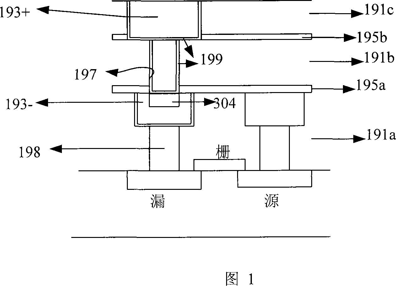
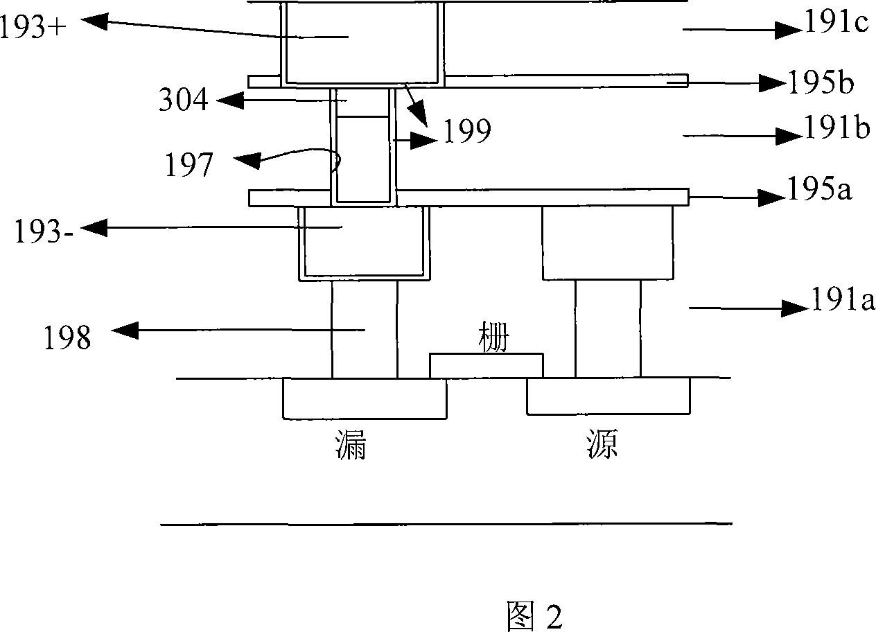
[0018] 1 and 2 are cross-sectional views according to one embodiment of the present invention. Figure 1 is Cu x The O storage medium 304 is directly below the through hole 197, and FIG. 2 is Cu x O The storage medium 304 is directly above the through hole 197. Wherein the lower dielectric layer 191a is formed on the semiconductor substrate (hereinafter referred to as the substrate), the lower plug 198 is patterned on the 191a and then etched until it penetrates 191a, exposing a predetermined area of the substrate, the lower dielectric layer 191a can be doped Silicon oxide layer, such as phosphorus or boron doped silicon oxide (BPSG) or phosphorus doped silicon oxide (PSG).
[0019] The lower plug 198 may be a conductive material, such as W, heavily doped polysilicon, or a conductive material containing N, such as TiN.
[0020] A cap layer 195 a , an insulating dielectric layer 191 b , an etching stop layer 195 b , and an insulating dielectric layer 191 c are covered seque...
PUM
 Abstract
Description
Claims
Application Information

