Package component

A technology for packaging components and components, which is applied in the field of semiconductor packaging components and can solve the problems of low heat dissipation efficiency

Inactive Publication Date: 2007-11-21
TAIWAN SEMICON MFG CO LTD
View PDF2 Cites 7 Cited by
  • Summary
  • Abstract
  • Description
  • Claims
  • Application Information

AI Technical Summary

Problems solved by technology

However, since such a heat dissipation layer or fan is not part of the structure of the packaged component, the efficiency of heat dissipation is relatively low.

Method used


Image

  • Package component
  • Package component
  • Package component

Examples


Embodiment Construction

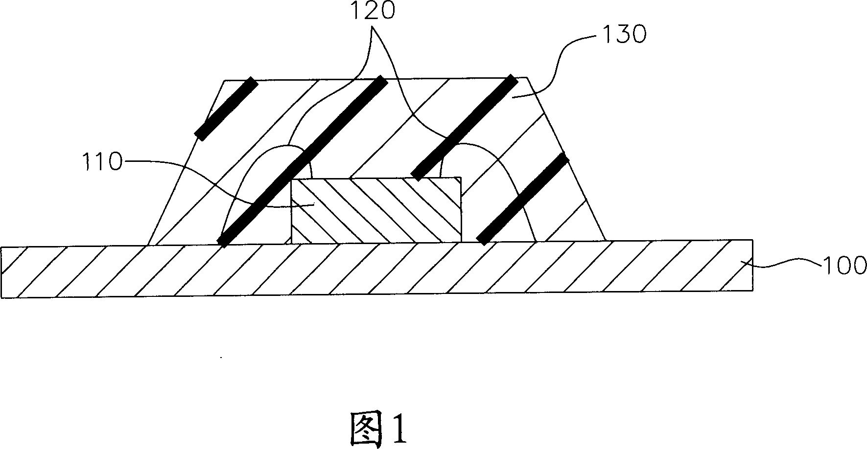
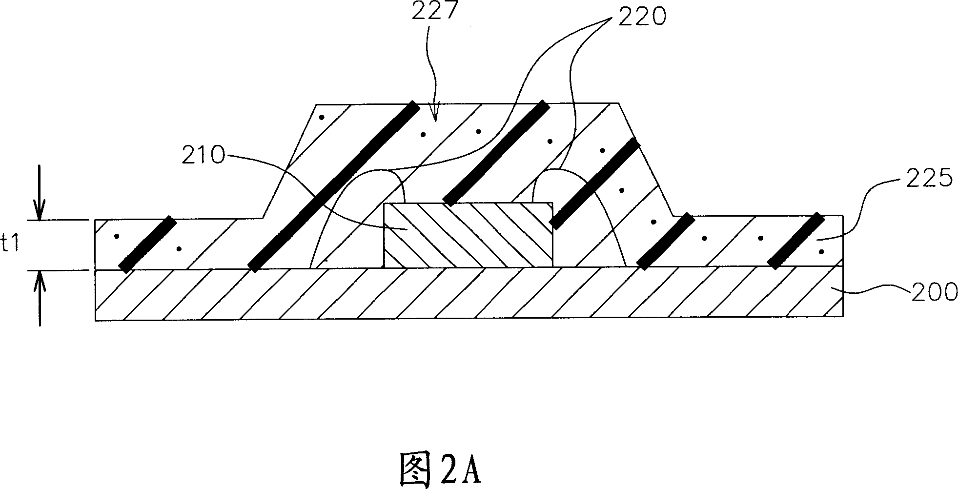
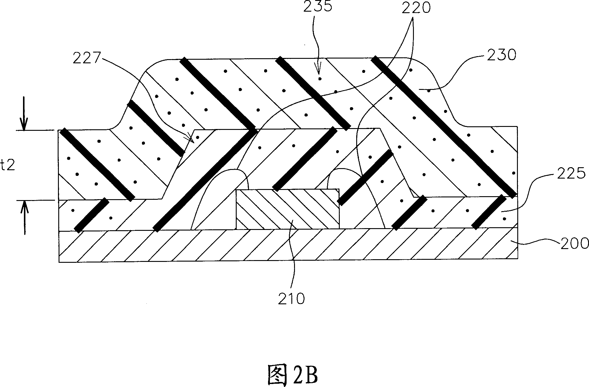
[0037] In order to further explain the technical means and effects of the present invention to achieve the intended purpose of the invention, the specific implementation, structure, features and effects of the packaging components proposed according to the present invention will be described in detail below in conjunction with the accompanying drawings and preferred embodiments. The description is as follows.

[0038] The following description of representative embodiments will be made in conjunction with the accompanying drawings. In descriptions, relative adjectives such as "lower", "higher", "horizontal", "vertical", "above", "below", "on", "below", " top", "bottom", etc., and similar adverbs (e.g., "horizontally", "vertically", "upwardly", "downwardly", etc.), should be used according to the following description or according to the figure in question Orientation shown.These relative terms are used for convenience of description and do not require precise orientation of t...


PUM


Abstract

Packaged devices and methods of forming packaged devices are provided. At least one device is disposed on a substrate. The material layer encapsulates the device and covers at least a portion of the substrate, wherein the material layer comprises at least a first portion adjacent to the device and a second portion over the first portion. The second portion has a thermal conductivity higher than a thermal conductivity of the first portion.

Description

technical field [0001] The invention relates to a semiconductor packaging component. Background technique [0002] In order to protect the chips cut from the wafer after the semiconductor manufacturing process, various device packaging methods and structures have been proposed. Packaged components protect the semiconductor components therein from particles, moisture, electric charges or other unexpected factors in the external environment, so as to improve the stability and working performance of the semiconductor components. [0003] FIG. 1 is a cross-sectional view of a prior art package. The packaging device includes a substrate 100 , a device 110 (ie, a semiconductor die or chip) and a protective epoxy resin layer 130 . The device 110 is disposed on the substrate 100 and electrically connected to the substrate 100 by gold wires 120 . The epoxy resin layer 130 covers the component 110 and dissipates the heat generated by the component 110 to a heat dissipation layer (n...

Claims


Application Information

Patent Timeline
Patent Type & Authority Applications(China)
IPC IPC(8): H01L23/29H01L23/373
CPCH01L2924/01019H01L2924/1815H01L23/3121H01L23/295H01L2924/1433H01L2224/45144H01L2924/01079H01L24/48H01L2924/3025H01L23/293H01L2224/48227H01L2924/07802H01L2224/45147H01L2224/45124H01L2924/12041H01L2924/14H01L2924/181H01L2924/00014H01L24/45H01L2924/00H01L2924/00015H01L2924/01029H01L2924/013H01L2924/00013H01L2924/00012H01L2224/45015H01L2924/207
Inventor 陈宪伟陈学忠郑义荣
Owner TAIWAN SEMICON MFG CO LTD
Why Eureka
Try Eureka