Printed circuit board
A technology of printed circuit substrate and base insulating layer, applied in the directions of printed circuit, printed circuit, printed circuit manufacturing, etc., can solve problems such as the reduction of electrical signal transmission efficiency
- Summary
- Abstract
- Description
- Claims
- Application Information
AI Technical Summary
Problems solved by technology
Method used
Image

Examples
no. 1 approach
[0028] (1) Manufacturing method of printed circuit board
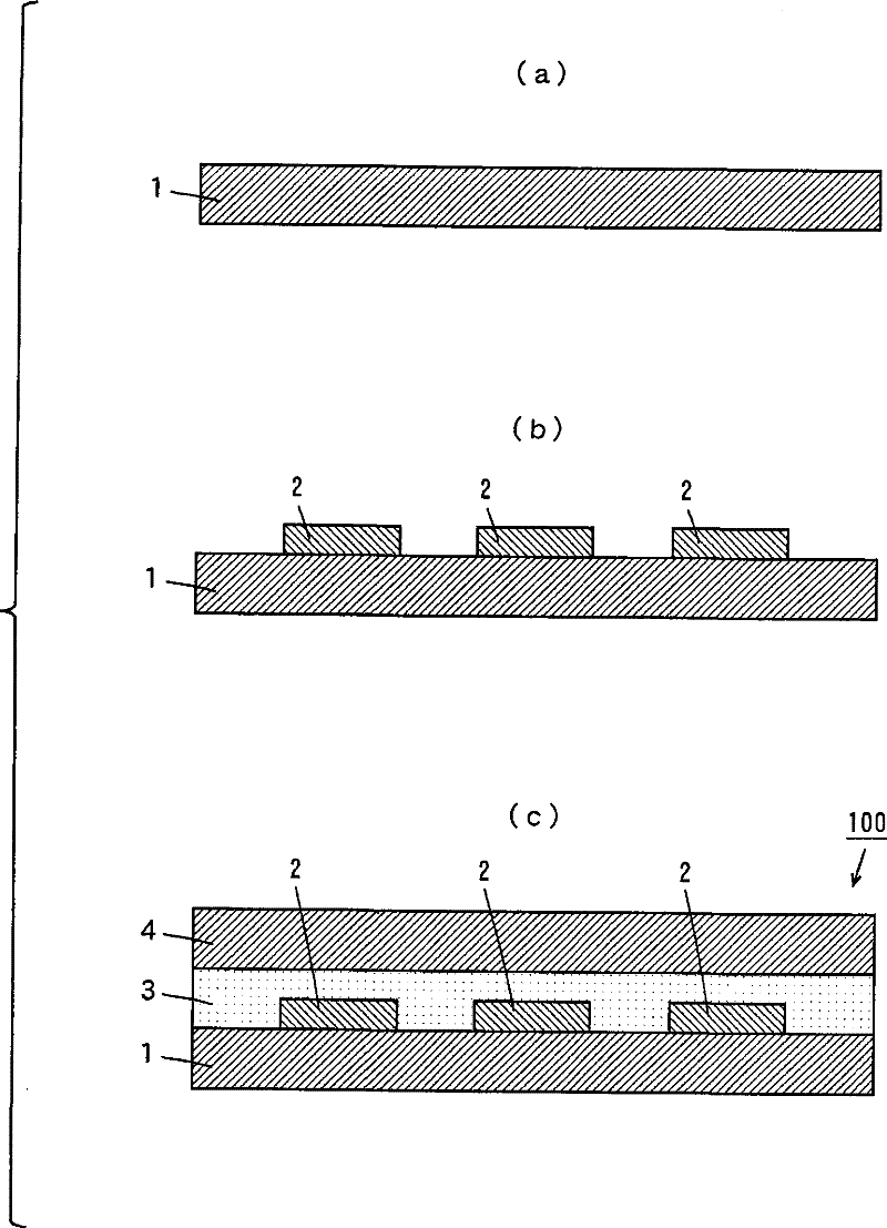
[0029] figure 1 It is a process cross-sectional view showing the manufacturing method of the printed circuit board which concerns on 1st Embodiment of this invention.
[0030] First, if figure 1 As shown in (a), an insulating base layer 1 is prepared. The insulating base layer 1 is made of, for example, polyimide. The thickness of the insulating base layer 1 is preferably not less than 5 μm and not more than 50 μm, more preferably not less than 10 μm and not more than 30 μm.
[0031] Next, if figure 1 As shown in (b), a plurality of conductor patterns (wiring patterns) 2 having a predetermined pattern are formed on the insulating base layer 1 by a well-known semi-additive method. Conductor pattern 2 is made of copper, for example. The thickness of the conductive pattern 2 is preferably not less than 5 μm and not more than 30 μm, more preferably not less than 8 μm and not more than 24 μm. In addition, the widt...
no. 2 approach
[0046] Figure 4 It is a cross-sectional view showing a printed circuit board according to a second embodiment of the present invention. The printed circuit board 200 of the second embodiment and figure 1 The printed circuit board 100 of (c) differs in the following points.
[0047] Such as Figure 4 As shown, in the printed circuit board 200 of this embodiment, the ground layer 5 is provided on the lower surface of the insulating base layer 1 . In addition, a cover insulating layer 7 is provided on the lower surface of the base insulating layer 1 so as to cover the ground layer 5 via the adhesive layer 6 .
[0048] Wherein, the ground layer 5, the adhesive layer 6 and the cover insulating layer 7 can be respectively used with figure 1 The conductive pattern 2, the adhesive layer 3 and the cover insulating layer 4 are formed by the same method and material. In addition, in this embodiment, the plurality of conductor patterns 2 are located inside the ground layer 5 in th...
Embodiment
[0061] Printed circuit boards of Examples and Comparative Examples were produced, and the characteristic impedance of the conductor pattern was measured.
[0062] (Example)
[0063] In the example, making Figure 4 The printed circuit substrate 200 is illustrated. Wherein, the thickness of the insulating base layer 1 is 25 μm, the width of the conductive pattern 2 is 40 μm, the thickness of the conductive pattern 2 is 10 μm, and the thickness of the insulating cover layer 4 is 12.5 μm.
PUM
 Abstract
Description
Claims
Application Information
 - R&D
- Intellectual Property
- Life Sciences
- Materials
- Tech Scout
- Unparalleled Data Quality
- Higher Quality Content
- 60% Fewer Hallucinations
Browse by: Latest US Patents, China's latest patents, Technical Efficacy Thesaurus, Application Domain, Technology Topic, Popular Technical Reports.
© 2025 PatSnap. All rights reserved.Legal|Privacy policy|Modern Slavery Act Transparency Statement|Sitemap|About US| Contact US: help@patsnap.com