Capacitive load driving circuit, capacitive load driving method, and driving circuit for liquid crystal display device

A capacitive load and drive circuit technology, applied to static indicators, instruments, etc., can solve problems such as charge pump failure, achieve the effects of saving power consumption, improving drive characteristics, and reducing costs

Inactive Publication Date: 2009-01-07
RENESAS ELECTRONICS CORP
View PDF2 Cites 34 Cited by
  • Summary
  • Abstract
  • Description
  • Claims
  • Application Information

AI Technical Summary

Problems solved by technology

Operating the second and third controllable switches to send a signal to turn on the second and fourth MOSFETs, thereby disabling the charge pump

Method used


Image

  • Capacitive load driving circuit, capacitive load driving method, and driving circuit for liquid crystal display device
  • Capacitive load driving circuit, capacitive load driving method, and driving circuit for liquid crystal display device
  • Capacitive load driving circuit, capacitive load driving method, and driving circuit for liquid crystal display device

Examples


no. 1 approach

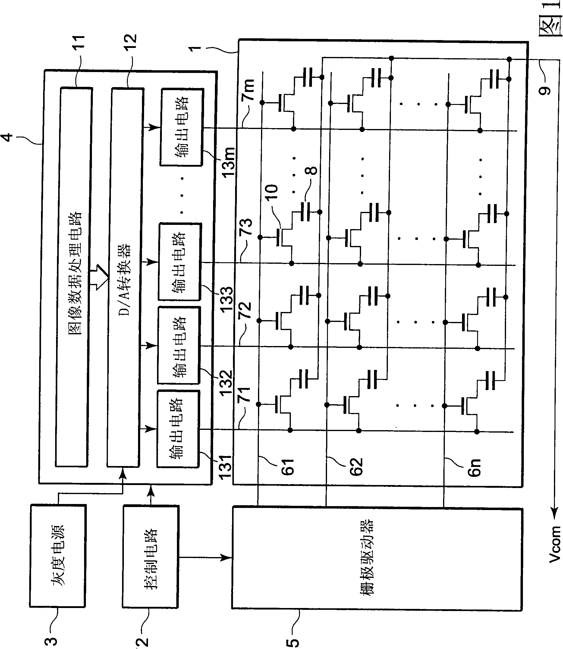
[0052] FIG. 1 is a block diagram showing the configuration of a liquid crystal display device according to a first embodiment of the present invention. The configuration of this liquid crystal display device is the same as that of the liquid crystal display device described in the section describing the prior art, but will be described again below. The liquid crystal display device according to the first embodiment has a system for applying an analog image data signal generated based on digital image data to a liquid crystal panel. The liquid crystal display device includes a liquid crystal panel 1 , a control circuit 2 , a grayscale power supply circuit 3 , a data electrode drive circuit (source driver) 4 and a scan electrode drive circuit (gate driver) 5 .

[0053] The liquid crystal display panel has an active matrix driving system using thin film transistors (TFTs) as switching elements. In the liquid crystal panel 1, the pixels are respectively composed of n (n is a natu...

no. 2 approach

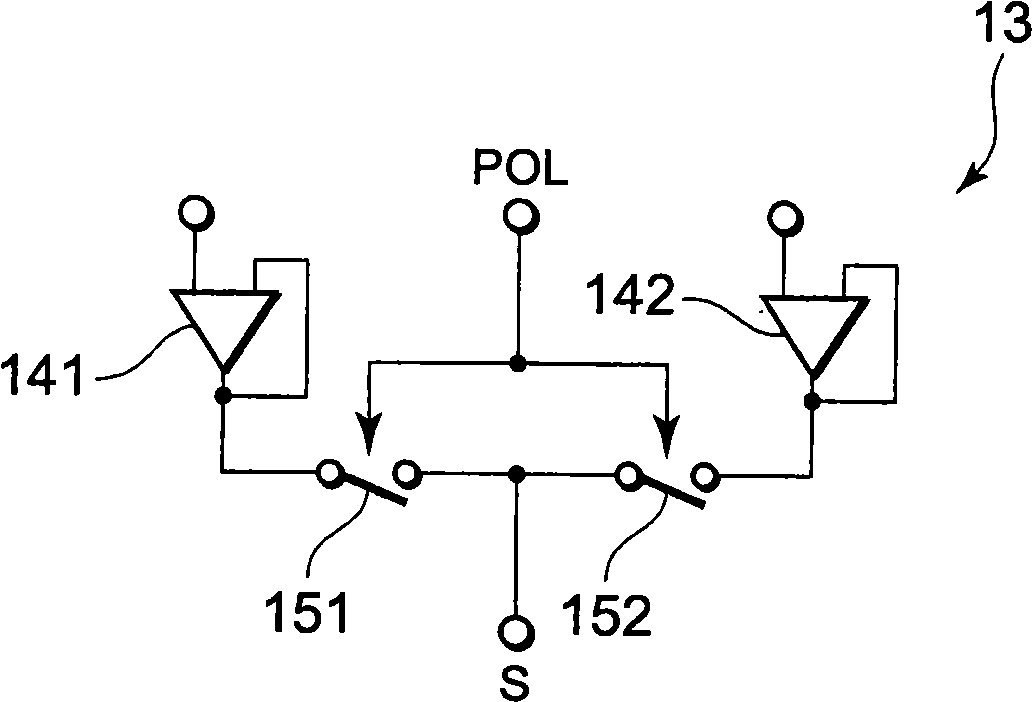
[0104] In the first embodiment as described above, the voltage used for the precharge of the arithmetic amplifier having the precharge (overdrive) function is determined as the positive power supply voltage (VDD) or the negative power supply voltage (VSS), and by changing the precharge Charging time is optimized for this drive. In the second embodiment, the precharge time is constant, and the driving is optimized by varying the precharge voltage (ie, a voltage different from the desired voltage). Since the difference from the first embodiment is only the output circuit 13, description of the liquid crystal display device as a whole will be omitted below.

[0105] Figure 17 One circuit of each of the digital-to-analog converter 12 and the output circuit 13 of the source driver 4 is shown. The output circuit 13 includes a most significant bit determination circuit 27 , a switch control circuit 30 , a precharge voltage control circuit 31 and an LCD drive amplifier circuit 60 ....


PUM


Abstract

The invention provides a drive circuit capable of applying improved drive performance and saving power consumption at same time. Capacitive load drive circuit comprises: grid drive, for driving scanning electrode aligned with row direction of capacitive load circuit installed in matrix; and a source drive, for driving digital electrode aligned with line direction of capacitive load circuit. The source drive comprises multiple output circuit aligned at line direction, for driving every data electrode. Every circuit of multiple output circuits changes precharging electric quantity at position of scanning electrode driven by the grid drive and then drives corresponding data electrode.

Description

technical field [0001] The present invention relates to a driving circuit and a driving method for driving a capacitive load, in particular to a driving circuit and a driving method for a liquid crystal display device, and the circuit and method are used for driving a capacitive load of a liquid crystal display panel or the like . Background technique [0002] In the current development, the size of the panels is further increased. In televisions in particular, this development is likely to continue, as evidenced by the fact that even LCD panels have been produced in sizes 50 inches or larger. However, as the size of the liquid crystal panel increases, the further increase of the load on the data line of the thin film transistor (TFT) leads to the problem that data cannot be written into the farthest data line within one horizontal period (1H period). In order to solve this problem, a measure (referred to as a "dual-row drive" system) has conventionally been taken in which...

Claims


Application Information

Patent Timeline
Patent Type & Authority Applications(China)
IPC IPC(8): G09G3/36
CPCG09G2330/021G09G3/3614G09G3/3688G09G2310/0248
Inventor 西村浩一
Owner RENESAS ELECTRONICS CORP
Why Eureka
Try Eureka