Testing method for badness of LCD critical point

A technology of liquid crystal display and testing method, which is applied in the directions of instruments, measuring electricity, measuring devices, etc., can solve the problems of poor deflection of liquid crystal molecules, poor electrical characteristics of thin film transistors, and difficult processes.

Inactive Publication Date: 2009-03-18
BOE TECH GRP CO LTD +1
View PDF0 Cites 9 Cited by
  • Summary
  • Abstract
  • Description
  • Claims
  • Application Information

AI Technical Summary

Problems solved by technology

[0003] In this way, although the actual working conditions can be simulated to the maximum extent, it cannot effectively detect a considerable number of defects close to the critical point, such as poor deflection of liquid crystal molecules, or poor electrical characteristics of thin-film transistors (TFTs), etc.
Since this bad phenomenon looms in the voltage environment of the critical point range, this part of the bad may not appear immediately at the initial detection, but after a period of use or when the external environment changes, this part of the bad will appear, which will cause Difficulties in subsequent processes, or losses to buyers

Method used


Image

  • Testing method for badness of LCD critical point
  • Testing method for badness of LCD critical point
  • Testing method for badness of LCD critical point

Examples


no. 1 example

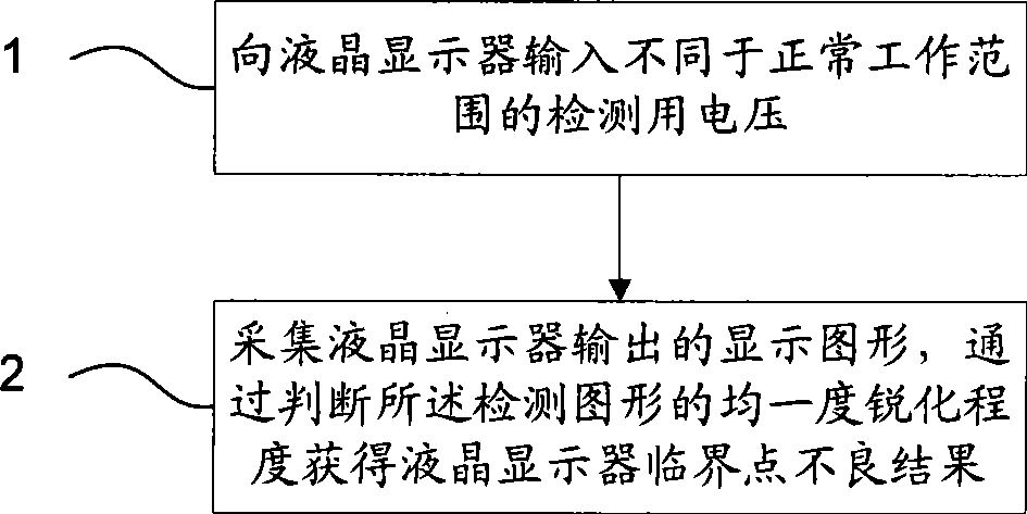
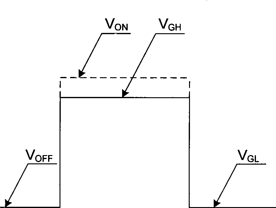
[0023] figure 2 It is a schematic diagram of the first embodiment of the present invention. The liquid crystal display critical point bad test method of this embodiment is specifically: to the liquid crystal display input detection grid forward open voltage V GH and sense the gate negative turn-off voltage V GL , where the detection gate forward turn-on voltage V GH Compared with the working gate positive full turn-on voltage V ON 20% to 50% lower, the gate negative turn-off voltage V for detection GL Equal to the full negative turn-off voltage of the working gate V OFF ; Gather the display graphics output by the liquid crystal display, and obtain the bad result of the critical point of the liquid crystal display by judging the uniformity sharpening degree of the detection graphics.

[0024] Specifically, before the test of this embodiment, it is necessary to modify the printed circuit board (PCB) of the signal input source of the liquid crystal display panel, and cut of...

no. 2 example

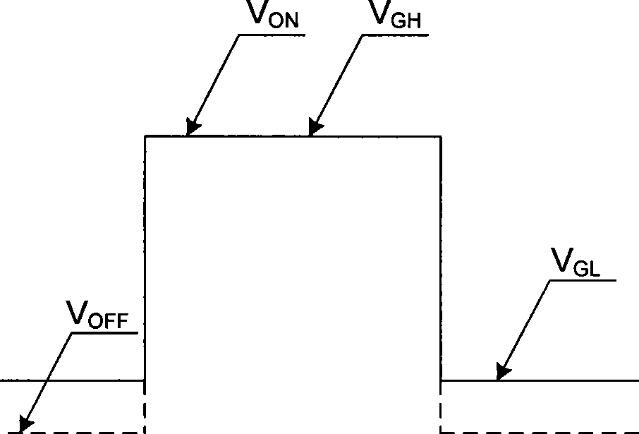
[0029] image 3 It is a schematic diagram of the second embodiment of the present invention. The liquid crystal display critical point bad test method of this embodiment is specifically: to the liquid crystal display input detection grid forward open voltage V GH and sense the gate negative turn-off voltage V GL , where the detection gate forward turn-on voltage V GH Equal to the working gate forward fully open voltage V ON , to detect the gate negative turn-off voltage V GL Compared with the working gate negative complete turn-off voltage V OFF 20% to 50% higher; collect the display graphics output by the liquid crystal display, and obtain the bad result of the critical point of the liquid crystal display by judging the uniformity sharpening degree of the detection graphics.

[0030] The specific process and working principle of the test in this embodiment are the same as those in the first embodiment. In this embodiment, the negative turn-off voltage V GL Compared with...

no. 3 example

[0033] Figure 4 It is a schematic diagram of the third embodiment of the present invention. The liquid crystal display critical point bad test method of this embodiment is specifically: to the liquid crystal display input detection grid forward open voltage V GH and sense the gate negative turn-off voltage V GL , where the detection gate forward turn-on voltage V CL Compared with the working gate positive full turn-on voltage V ON 20% to 50% lower, the gate negative turn-off voltage V for detection GL Compared with the working gate negative complete turn-off voltage V OFF 20% to 50% higher; collect the display graphics output by the liquid crystal display, and obtain the bad result of the critical point of the liquid crystal display by judging the uniformity sharpening degree of the detection graphics.

[0034] The specific testing process and working principle of this embodiment are the same as those of the first embodiment, and will not be repeated here. The gate forw...


PUM


Abstract

The invention relates to a liquid crystal display device critical point disability test method, comprising the steps of: inputting a check voltage different from a normal working range into a liquid crystal display device; collecting the display picture output by the liquid crystal display device, and judging the uniformity sharpening degree of the check image to obtain the liquid crystal display device critical point disability result. The invention inputs a check voltage different from a normal working range, to represent the electric disability and visual disability of difficult discovery, thereby effectively detecting the critical point disability of a liquid crystal display device.

Description

technical field [0001] The invention relates to a liquid crystal display testing method, in particular to a liquid crystal display critical point defect testing method. Background technique [0002] Liquid crystal displays need to undergo strict testing before leaving the factory, for example, conventional electrical signal pattern testing is required in the liquid crystal display testing stage. The electrical signal used by the conventional electrical signal pattern detection method is generally a conventional signal program set in accordance with the VESA standard. The working state is deflected. [0003] Although this can simulate the actual working conditions to the maximum extent, it cannot effectively detect a considerable number of defects close to the critical point, such as poor liquid crystal molecule deflection, or poor electrical characteristics of thin-film transistors (TFTs). Since this bad phenomenon looms in the voltage environment of the critical point ran...

Claims


Application Information

Patent Timeline
Patent Type & Authority Applications(China)
IPC IPC(8): G02F1/13G01R31/00
Inventor 徐涛
Owner BOE TECH GRP CO LTD
Why Eureka
Try Eureka