Supercharge Your Innovation With Domain-Expert AI Agents!

Input circuit

An input circuit, input terminal technology, applied in the direction of logic circuit connection/interface arrangement, logic circuit coupling/interface using field effect transistors, etc., can solve the problem that the threshold voltage of the buffer G1 cannot be reached, cannot be operated, and cannot be directly supplied. to buffers, etc.

Active Publication Date: 2009-04-15
WINBOND ELECTRONICS CORP
View PDF0 Cites 5 Cited by
  • Summary
  • Abstract
  • Description
  • Claims
  • Application Information

AI Technical Summary

Problems solved by technology

[0003] However, since the highest voltage level of the internal input voltage VINN is affected by the NMOS transistor NM1, it is limited to VDDIO-VthN, where VthN is the threshold voltage of the NMOS transistor NM1
Therefore, the voltage level of the high external input voltage (such as VDDIO) cannot be directly supplied to the buffer G1
In addition, the conventional input circuit 100 cannot operate at a relatively low input / output power supply voltage VDDIO
To be more clear, if the input / output supply voltage VDDIO is quite low, the internal input voltage VINN cannot reach the threshold voltage of the buffer G1

Method used


Image

  • Input circuit
  • Input circuit
  • Input circuit

Examples


Embodiment Construction

[0029] In order to make the above-mentioned features and advantages of the present invention more comprehensible, a detailed description will be given below of preferred embodiments in conjunction with the accompanying drawings.

[0030] Reference will now be made in detail to this embodiment of the present invention, and examples of this embodiment are illustrated in the accompanying drawings. Wherever possible, the same reference numbers are used in the drawings and embodiments to represent the same or similar parts.

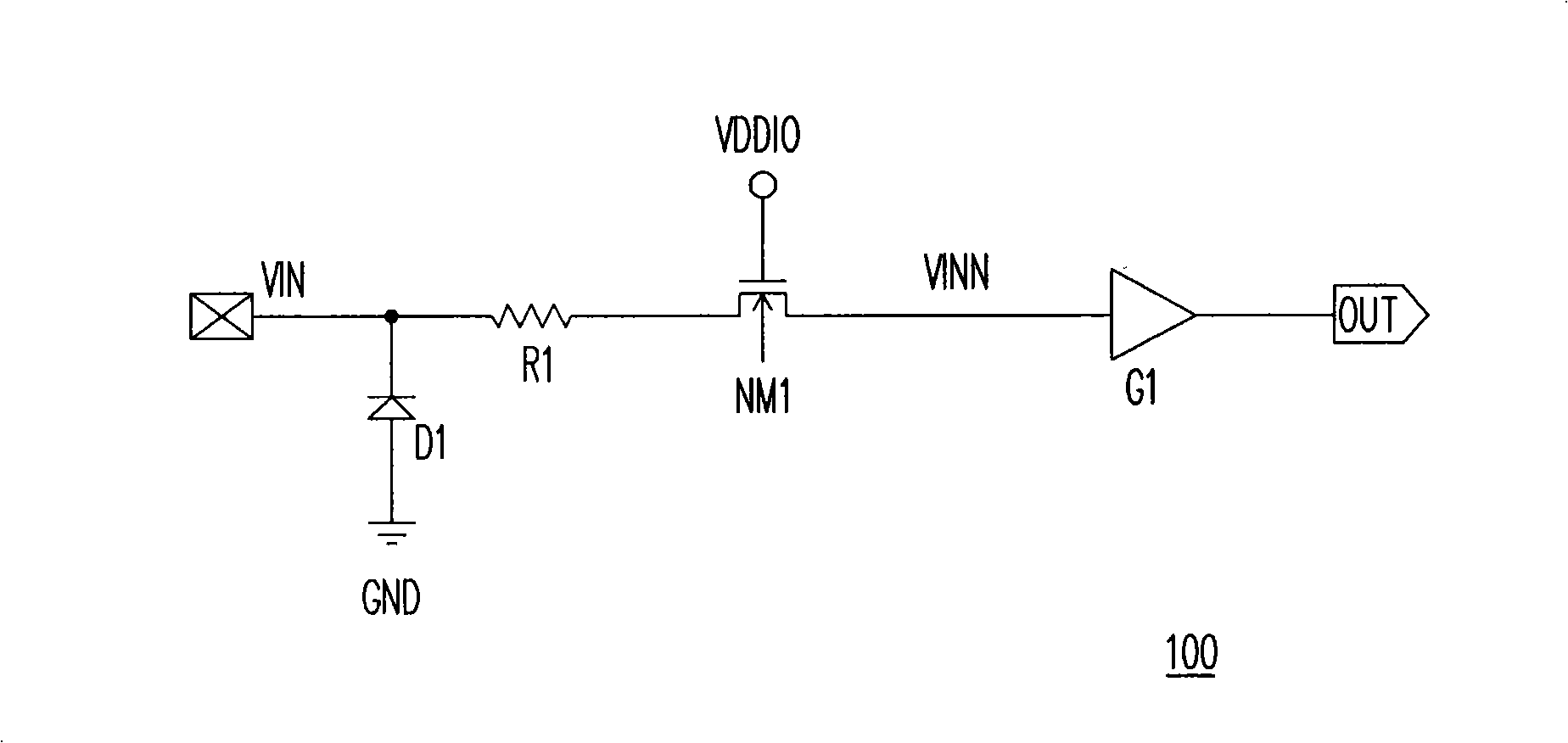
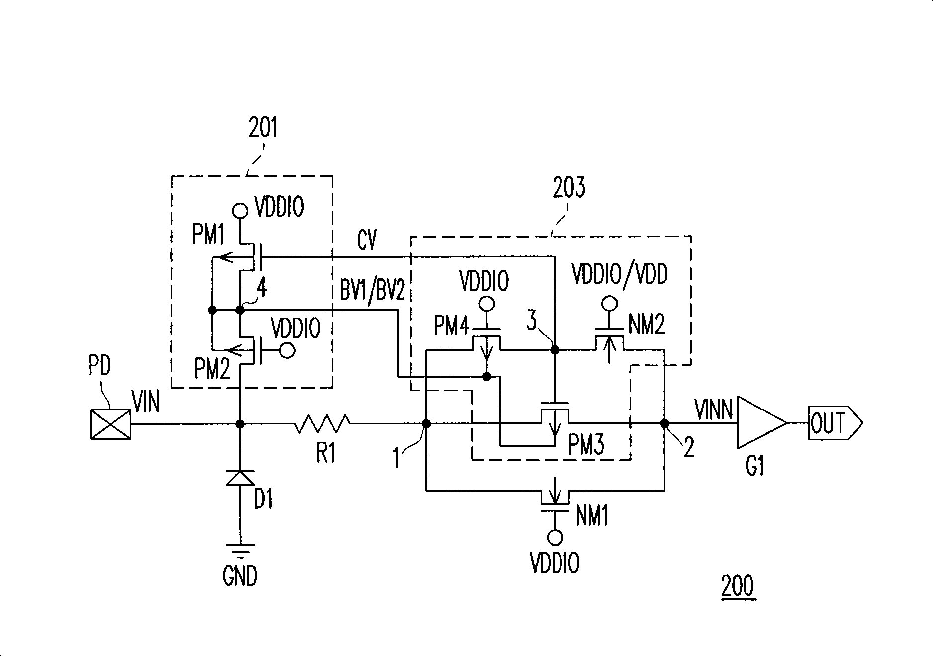
[0031] figure 2 Shown is a circuit diagram of the input circuit 200 according to an embodiment of the present invention. Please refer to figure 2 The input circuit 200 of this embodiment includes a diode D1, a resistor R1, a first NMOS transistor NM1, a buffer G1, a base voltage generating unit 201, and an enhancement unit 203. In this embodiment, the diode D1 is an electrostatic discharge protection element, and the diode D1 has an anode and a cathode. The ano...


PUM


Abstract

The invention provides an input circuit which comprises a diode, a resistance, a first transistor, a buffer, a matrix voltage generating unit and a strengthening unit. When an external input voltage is less than or equal to a first supply voltage (like an input / output supply voltage), the input circuit can utilize the matrix generating unit and the strengthening unit to lead an internal input voltage to be the same as the external input voltage. Furthermore, the input circuit can operate correctly even if the first supply voltage is extremely low. Therefore, the input circuit can be operated at the extremely low input / output supply voltage.

Description

Technical field [0001] The present invention relates to an input circuit, and more particularly, to a high-voltage-resistant input circuit having an extremely low input / output power supply voltage. Background technique [0002] figure 1 Shown is a circuit diagram of a traditional high-voltage withstand input circuit 100. Please refer to figure 1 The conventional input circuit 100 includes a diode D1, a resistor R1, an NMOS transistor NM1, and a buffer G1. Generally speaking, the diode D1 is an electrostatic discharge (ESD) protection element. The resistor R1 protects the NMOS transistor NM1 and the buffer G1 by increasing the delay, and reduces the noise intensity of the external input voltage VIN. The gate terminal of the NMOS transistor NM1 is biased at the input / output power supply voltage VDDIO, so that the NMOS transistor NM1 receives the external input voltage VIN and outputs the internal input voltage VINN to the buffer G1. [0003] However, the maximum voltage level of...

Claims


Application Information

Patent Timeline
IPC IPC(8): H03K19/0185
Inventor 小池秀治
Owner WINBOND ELECTRONICS CORP
Features
  • R&D
  • Intellectual Property
  • Life Sciences
  • Materials
  • Tech Scout
  • Unparalleled Data Quality
  • Higher Quality Content
  • 60% Fewer Hallucinations
Learn More