
Antenna arrangement and use thereof

A technology of antenna configuration and antenna structure, which is applied to antennas, antenna supports/installation devices, loop antennas, etc., and can solve problems such as antenna power loss

Inactive Publication Date: 2009-06-17
POLYIC
View PDF1 Cites 5 Cited by
  • Summary
  • Abstract
  • Description
  • Claims
  • Application Information

AI Technical Summary

Problems solved by technology

[0005] However, it has been found that in the region of the conductive layer remaining on the electrically insulating carrier substrate and adjacent to the antenna structure, during electrical operation of the antenna structure, electrical effects occur which lead to a power loss of the antenna

Method used


Image

  • Antenna arrangement and use thereof
  • Antenna arrangement and use thereof
  • Antenna arrangement and use thereof

Examples


Embodiment Construction

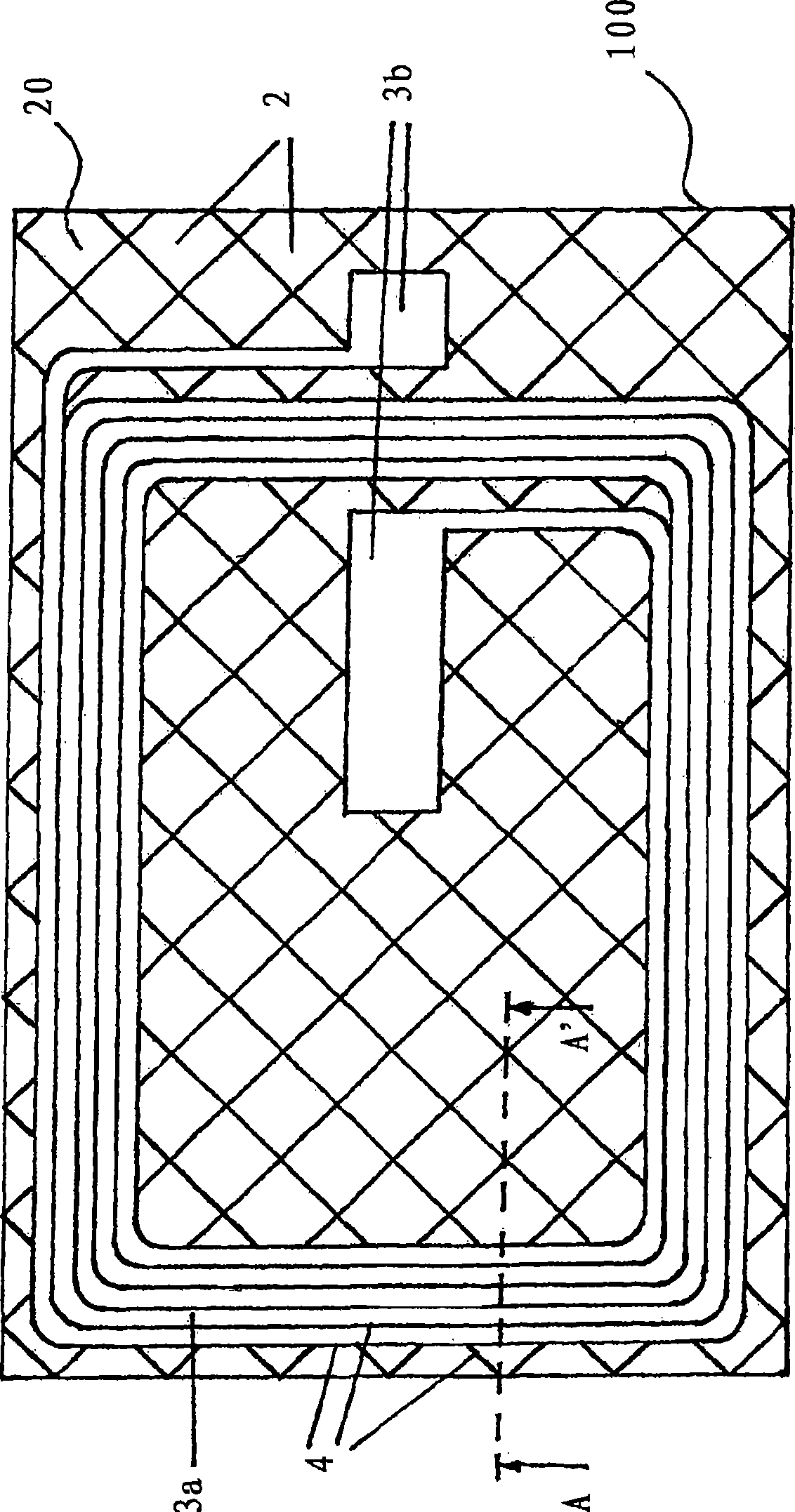
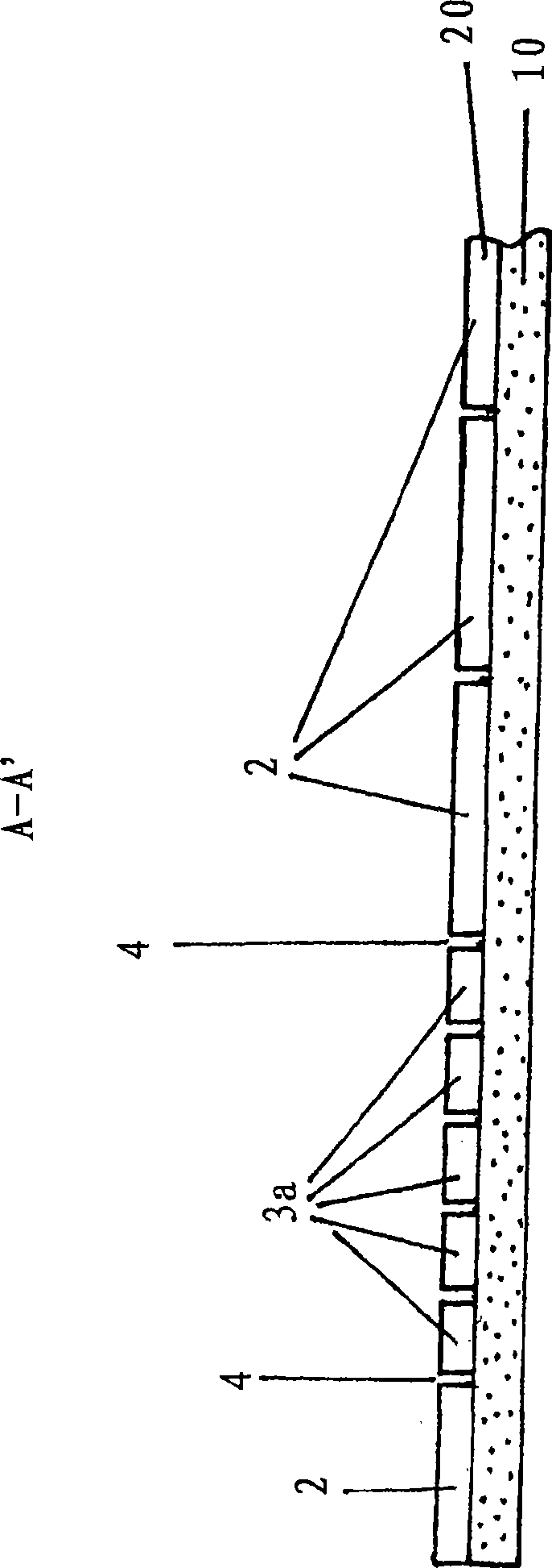
[0059] Figure 1a Antenna arrangement 100 is shown in plan view with respect to conductive layer 20 made of copper. The conductive layer 20 is structured by stamping and subsequent etching, forming the antenna structure 3a in the form of a helix with electrical contact areas 3b. Also by embossing and subsequent etching, the regions of the conductive layer 20 arranged inside the antenna structure 3 a and outside the latter are subdivided into parallelogram-shaped island regions 2 which are electrically insulated from one another. An insulating trench 4 is formed between the island region 2 and the antenna structure 3a and the contact region 3b (see also Figure 1b ). This type of insulating trench 4 is also provided between the individual turns of the antenna structure 3a.

[0060] Figure 1b Section A-A' shows the Figure 1a An area of ​​100 antenna configurations. This illustration also shows a carrier substrate 10 formed from a PET film with a thickness of 12 μm, on wh...


PUM

PropertyMeasurementUnit
thicknessaaaaaaaaaa
thicknessaaaaaaaaaa
thicknessaaaaaaaaaa

Abstract

The invention relates to an antenna configuration that has at least one electrically isolating carrier substrate and at least one electrically conductive layer applied to at least one side of the carrier substrate, with the electrically conductive layer having a first surface area and a second surface area, wherein the first surface area of the electrically conductive layer has the form of at least one antenna structure. The at least one antenna structure is electrically isolated from the second surface area of the electrically conductive layer and the second surface area of the electrically conductive layer is divided into island areas electrically isolated from one another at least in regions directly adjacent to the at least one antenna structure. The at least one antenna configuration can be used for contactlessly coupled transponders, in particular for RFID tags or Smart tags.

Description

technical field [0001] The invention relates to an antenna arrangement comprising at least one electrically insulating carrier substrate and at least one electrically conductive layer applied on at least one side of the carrier substrate. The invention also relates to the use of this antenna arrangement. Background technique [0002] Such an antenna arrangement for smart cards is known from DE 196 29 269 A1. Here, the antenna structure is produced by etching a conductive layer which is arranged on an electrically insulating plastic layer and printed with an etch-resistant photoresist in areas. In the regions of the conductive layer not coated with photoresist, said layer is removed by etching, the regions of the conductive layer covered with photoresist in the form of conductor tracks or antenna structures remain in the on the plastic layer. Then, if appropriate, the photoresist is removed and the antenna structure is covered with a protective varnish. [0003] Such meth...

Claims


Application Information

Patent Timeline
Patent Type & Authority Applications(China)
IPC IPC(8): H01Q7/00H01Q1/22G06K19/077
CPCH01Q7/00H01Q1/2225G06K19/07783G06K19/07749G06K19/07779Y10T29/49018G06K19/077H01Q1/22
Inventor J·菲柯尔H·维尔德W·克莱门斯W·莱博格M·洛伦茨
Owner POLYIC
Learn More