Touch panel

A technology of touch panel and transparent substrate, which is applied in the direction of instruments, electrical digital data processing, and input/output process of data processing, etc. It can solve the problems of poor conductivity of polymer conductive film 212, reliability of line drawing signal drift, surface Problems such as high contact resistance, to achieve good display tone, avoid linear drift phenomenon, and good flexibility

Inactive Publication Date: 2009-09-02
WINTEK CORP
View PDF0 Cites 11 Cited by
  • Summary
  • Abstract
  • Description
  • Claims
  • Application Information

AI Technical Summary

Problems solved by technology

like figure 2 The design of the polymer conductive film 212 formed on the transparent substrate 210 has better flexibility, and will not change the color tone of the image due to the yellowish color, and because the normal pressure coating process is adopted, the cost is relatively low. figure 1 The known design shown is low; however, the conductive polymer film 212 has inherently poor conductivity and high surface contact resistance, which will cause line drawing signal drift and poor reliability when applied to touch panel products The problem

Method used


Image

  • Touch panel
  • Touch panel
  • Touch panel

Examples


Embodiment Construction

[0040] Other purposes and advantages of the present invention can be further understood from the technical features disclosed in the present invention. In order to make the above and other objects, features and advantages of the present invention more comprehensible, the following specific embodiments are described in detail with reference to the accompanying drawings.

[0041] The above and other technical contents, features and effects of the present invention will be clearly presented in the following detailed description of the embodiments with reference to the accompanying drawings. The directional terms mentioned in the following embodiments, such as: up, down, left, right, front or back, etc., are only directions referring to the attached drawings. Accordingly, the directional terms are used to illustrate and not to limit the invention.

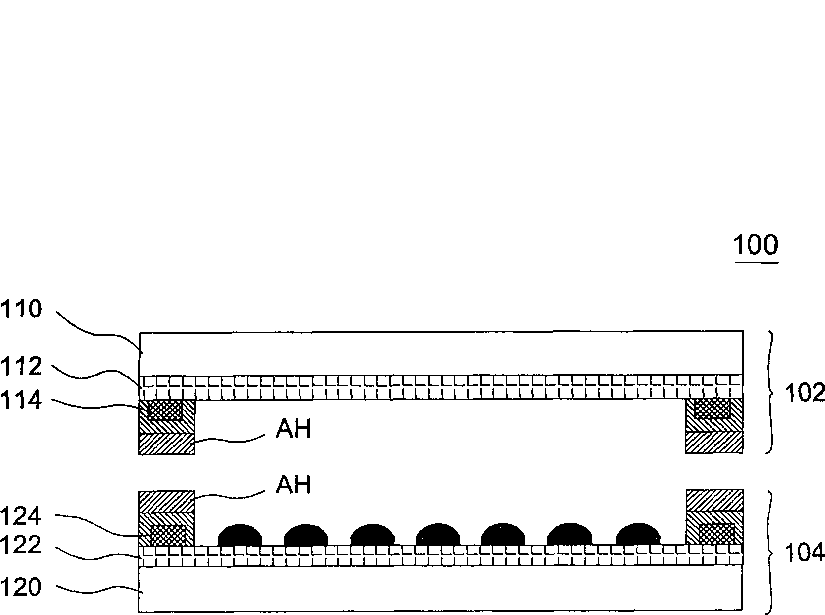
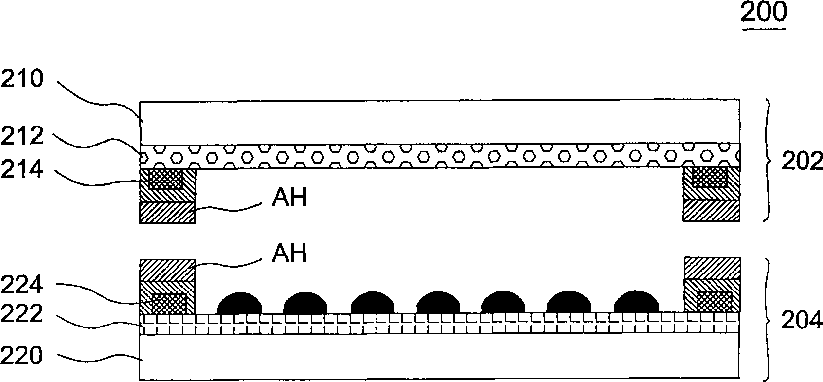
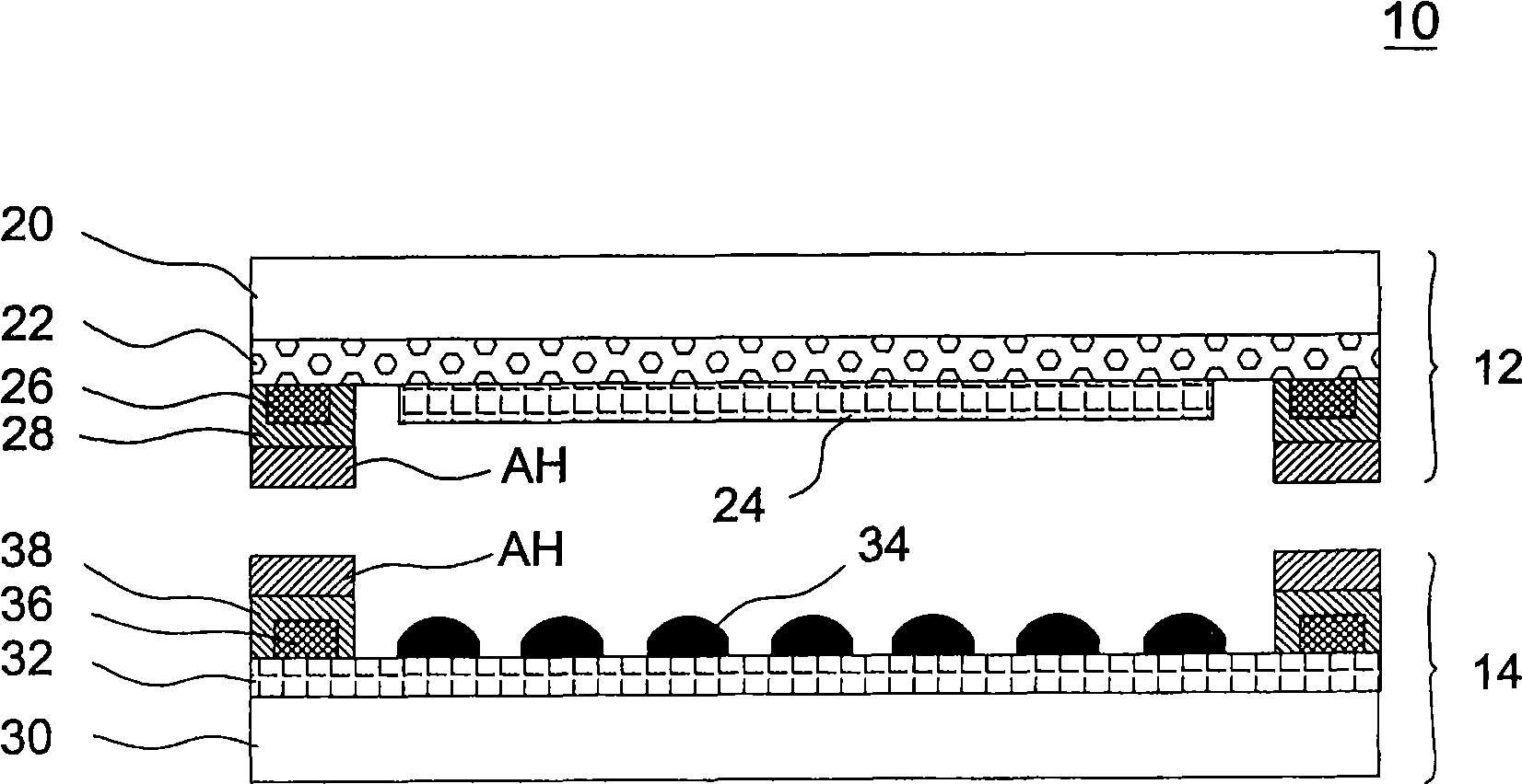
[0042] image 3 A schematic diagram of the design of the touch panel 10 according to an embodiment of the present invention is show...


PUM


Abstract

A touch panel is provided, comprising a first and a second electrode substrates opposite to one another and jointed by an adhesive to keep a gap. The first or second electrode substrate is provided with a composite transparent conductive layer having a polymeric conductive film and a non-polymeric conductive film bonded with each other to provide better flexibility and increase the drawable time of line, wherein the non-polymeric conductive film is capable of increasing the conductivity and reducing the surface contact impedance.

Description

technical field [0001] The present invention relates to a touch panel, in particular to a touch panel with an improved structure of a transparent conductive film with good properties. Background technique [0002] figure 1 It is a schematic diagram showing a conventional touch panel 100 design. Such as figure 1 As shown, the touch panel 100 includes an upper electrode substrate 102 and a lower electrode substrate 104 oppositely arranged, the upper electrode substrate 102 includes a transparent substrate 110, an ITO conductive film 112 and a signal transmission line 114 formed on the transparent substrate 110, the lower The electrode substrate 104 includes a transparent substrate 120 , an ITO conductive film 122 and signal transmission lines 124 formed on the transparent substrate 120 , and the upper electrode substrate 102 and the lower electrode substrate 104 can be joined by an adhesive AH. [0003] Such as figure 1 According to the design, the ITO conductive films 112...

Claims


Application Information

Patent Timeline
Patent Type & Authority Applications(China)
IPC IPC(8): G06F3/041C08L65/00C08L25/06C08L101/02C08K3/04C08K3/08
CPCG06F3/045
Inventor 王志源周承毅李俊贤
Owner WINTEK CORP
Why Eureka
Try Eureka