Signal conduction element

A conduction and signal technology, applied in the direction of electrical connection of printed components, printed circuit components, multi-layer circuit manufacturing, etc., can solve problems such as rising manufacturing costs and reduced operating efficiency of circuit boards, and achieve the effect of avoiding abnormal functions

Inactive Publication Date: 2009-12-02
计正斌
View PDF0 Cites 2 Cited by
  • Summary
  • Abstract
  • Description
  • Claims
  • Application Information

AI Technical Summary

Problems solved by technology

From the common four-layer, six-layer, eight-layer of traditional circuit boards, and even increased to more than ten layers, as the number of layers increases, the operation efficiency of the circuit board decreases and the manufacturing cost increases exponentially.

Method used


Image

  • Signal conduction element
  • Signal conduction element

Examples


Embodiment Construction

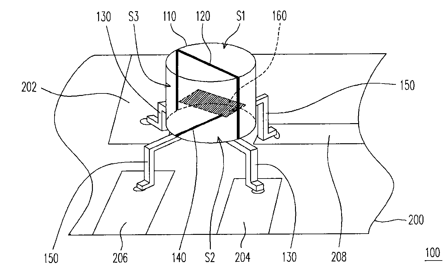
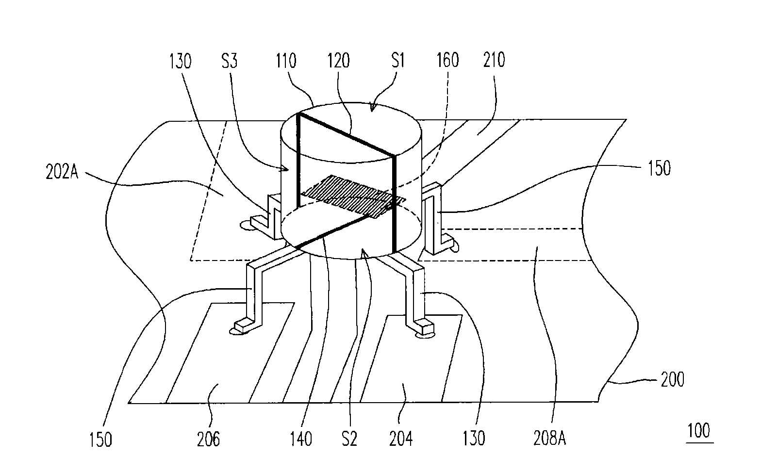
[0022] figure 1 It is a schematic diagram of a signal pass element 100 according to the first embodiment of the present invention. figure 2 It is a schematic diagram of a signal conducting element 100 connecting different layers of circuits on a circuit board according to the second embodiment of the present invention.

[0023] Please refer to figure 1 The signal conducting element 100 includes an insulator 110 , at least one first bridge wire 120 and at least one second bridge wire 140 , a plurality of first pins 130 and a plurality of second pins 150 . The signal conducting element 100 is suitable to be disposed on a circuit board 200 , and the circuit board 200 has a first circuit 202 , a second circuit 204 , a third circuit 206 and a fourth circuit 208 which are separated. In order to enable the signal conduction element 100 to connect the four separate lines smoothly, the second bridging line 140 is first arranged on the lower surface S2, and the first bridging line 12...


PUM


Abstract

The invention discloses a signal conduction element suitable for being arranged on a circuit board, comprising an insulator, at least one first bridging line, at least one second bridging line, a plurality of first pins and a plurality of second pins, wherein the first bridging line and the second bridging line are respectively arranged on different layers of the insulator; the first pins are electrically connected with two ends of the first bridging line, while the second fins are electrically connected with two ends of the second bridging line.

Description

technical field [0001] The present invention relates to an electronic component, and in particular to a signal conducting component. Background technique [0002] With the development of electronic devices towards light, thin, small and multi-functional, the requirements for internal electronic circuits are becoming more and more complex. In order to meet the above requirements, the area of ​​circuit boards is often made smaller and smaller, and the circuits on it are more and more complicated. The denser it is, and in order to meet the multi-faceted functional requirements of electronic products, and to achieve the maximum function with the most streamlined circuit distribution, in this case, the multi-layering of circuit boards is inevitable. [0003] On the other hand, with the diversification of electronic products, circuit designers often need to make large changes to the circuit designed in the early stage due to different functional requirements in the early stage and...

Claims


Application Information

Patent Timeline
IPC IPC(8): H05K1/11H05K3/46
Inventor 叶志刚丁晓娇范文纲
Owner 计正斌
Why Eureka
Try Eureka