

Signal conduction element
A conduction and signal technology, applied in the direction of electrical connection of printed components, printed circuit components, multi-layer circuit manufacturing, etc., can solve the problems of rising manufacturing costs and reduced operating efficiency of circuit boards, and achieve the effect of avoiding abnormal functions
- Summary
- Abstract
- Description
- Claims
- Application Information
AI Technical Summary
Problems solved by technology
Method used
Image

Examples
Embodiment Construction
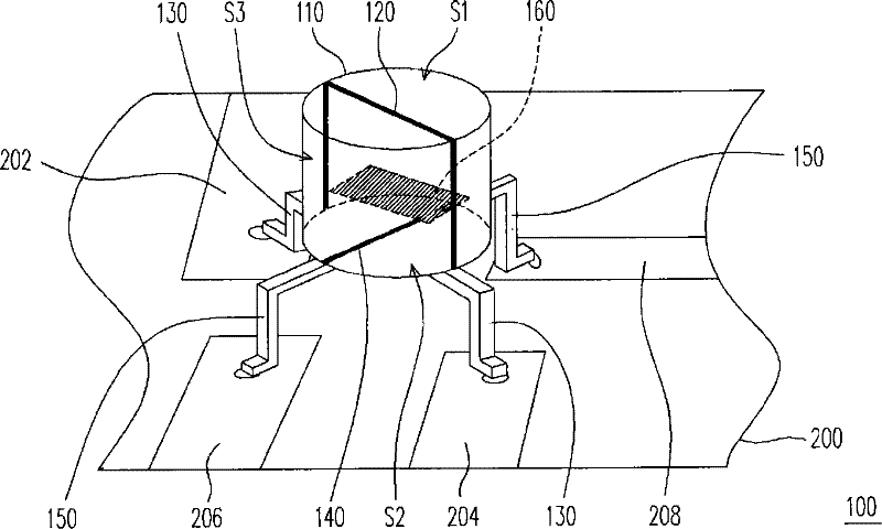
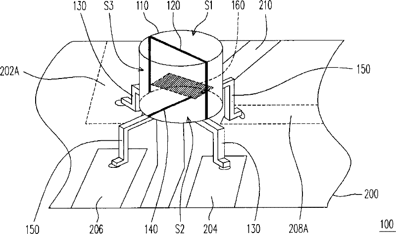
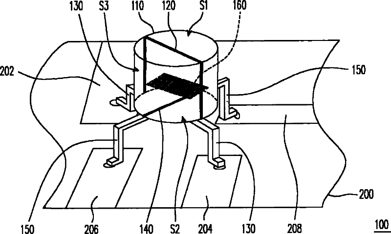
[0022] figure 1 It is a schematic diagram of a signal pass element 100 according to the first embodiment of the present invention. figure 2 It is a schematic diagram of a signal conducting element 100 connecting different layers of circuits on a circuit board according to the second embodiment of the present invention.
[0023] Please refer to figure 1 The signal conducting element 100 includes an insulator 110 , at least one first bridge wire 120 and at least one second bridge wire 140 , a plurality of first pins 130 and a plurality of second pins 150 . The signal conducting element 100 is suitable to be disposed on a circuit board 200 , and the circuit board 200 has a first circuit 202 , a second circuit 204 , a third circuit 206 and a fourth circuit 208 which are separated. In order to enable the signal conduction element 100 to connect the four separate lines smoothly, the second bridging line 140 is first arranged on the lower surface S2, and the first bridging line 12...
PUM
 Abstract
Description
Claims
Application Information