Method for introducing PCB design document from schematic diagram

A technology for designing documents and schematic diagrams, applied in computing, electrical digital data processing, special data processing applications, etc., can solve problems such as layout troubles, reduce work efficiency, and spend a lot of time, and achieve the effect of avoiding the reduction of electrical performance

Inactive Publication Date: 2010-02-03
SHANGHAI WINGTECH ELECTRONICS TECH
View PDF3 Cites 17 Cited by
  • Summary
  • Abstract
  • Description
  • Claims
  • Application Information

AI Technical Summary

Problems solved by technology

This method causes a large number of components to be arranged in disorder, and it takes a lot of time to sort them out, causing troubles to the later layout and reducing work efficiency.

Method used


Image

  • Method for introducing PCB design document from schematic diagram

Examples


Embodiment Construction

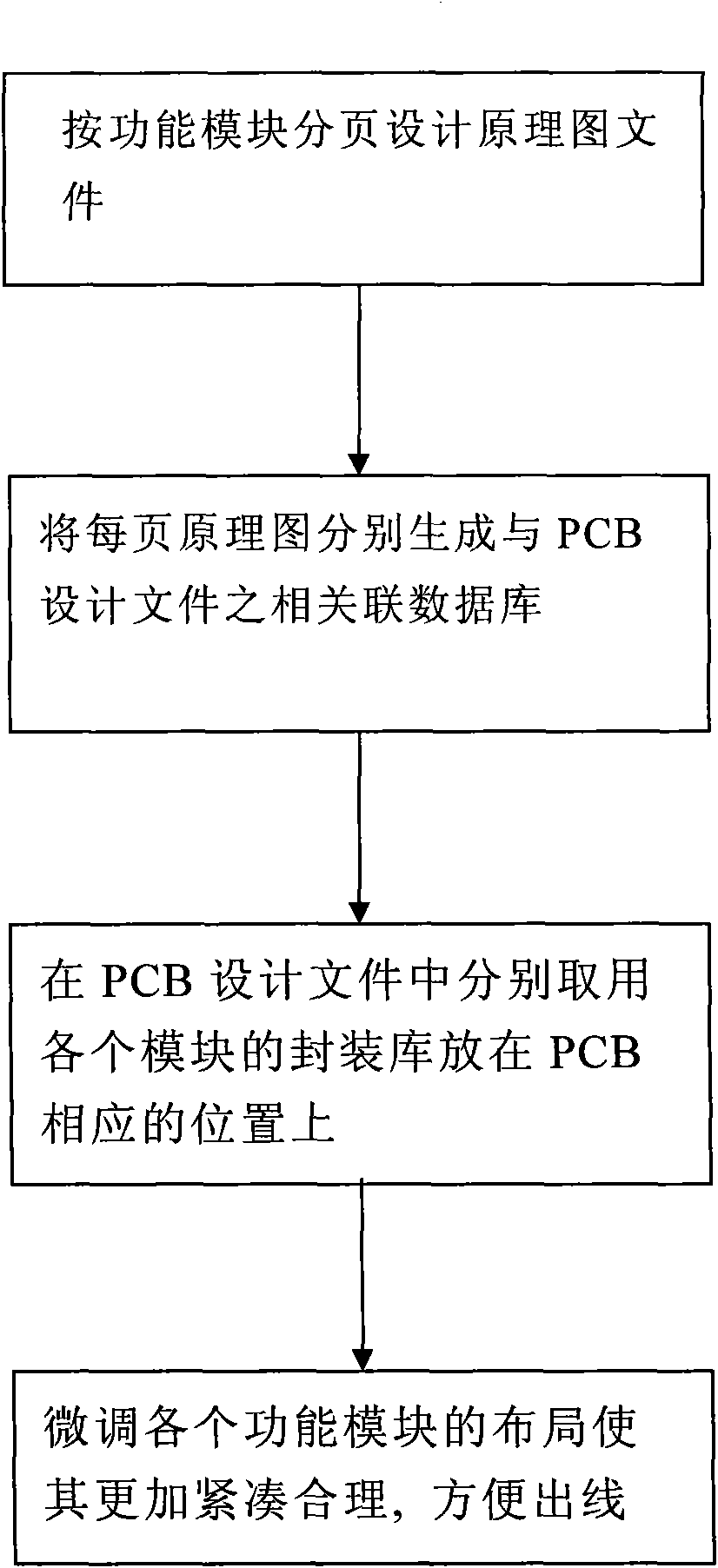
[0015] Such as figure 1 As shown, the present invention provides a kind of method that imports PCB design file from schematic diagram, comprises the following steps:

[0016] a: Carry out modular design in accordance with the realized functions in the schematic design file, that is to say, make the circuit design of the same functional module in the same schematic diagram, and place them in the corresponding positions according to the connection relationship. The module includes the main chip and the corresponding peripheral circuits;

[0017] b: Generate the database associated with the PCB design file for each functional module of the schematic diagram, and generate the files associated with the PCB in units of functional modules for the designed schematic diagram;

[0018] c: In the PCB design file, the associated files generated according to the schematic diagram are used to call the corresponding functional modules in the package library and placed in the appropriate po...


PUM


Abstract

The invention discloses a method introducing PCB design document from a schematic diagram. The method comprises: performing modular design according to realized function in a schematic diagram designdocument; according to a schematic diagram functional module, respectively and independently associating to the PCB design document; in the PCB design document, respectively according to relevant document generated by the schematic diagram, calling each corresponding functional module from a packaging library in the PCB design document, and putting to the proper position in the PCB design document; trimming to form component position of each functional module to cause the component to be regular and convenient for routing. The invention can shorten time of laying later-stage circuit board components and lower the ratio of making mistakes in the subsequent process of putting components.

Description

technical field [0001] The invention relates to a method for importing PCB design files from schematic diagrams. Background technique [0002] As the function, performance and design cycle requirements of electronic products are getting higher and higher, the electronic design is becoming more and more complex, and the number of components used in the design is also increasing geometrically. At present, the principle of first completeness is generally adopted Figure 1 Generate the netlist once and associate it with the PCB design file, and then refer to the schematic diagram for layout. This method causes a large number of components to be arranged in disorder, and it takes a lot of time to sort them out, causing troubles in the later layout and reducing work efficiency. Therefore, how to correctly and quickly layout according to the connection relationship of the schematic diagram is particularly important. Contents of the invention [0003] The technical problem to be...

Claims


Application Information

Patent Timeline
Patent Type & Authority Applications(China)
IPC IPC(8): G06F17/50
Inventor 曾明洋陈贤能
Owner SHANGHAI WINGTECH ELECTRONICS TECH
Why Eureka
Try Eureka