
Optical input preamplifier for optical communication receiver
A preamplifier and receiver technology, applied in the field of optical communication reception, can solve the problems of difficult-to-burst signal reception amplification, response delay and low reception sensitivity, and achieve high open-loop gain and bandwidth, high optical reception sensitivity, and reduced response time. delayed effect
- Summary
- Abstract
- Description
- Claims
- Application Information
AI Technical Summary
Problems solved by technology
Method used
Image


Examples
Embodiment Construction
[0033] Preferred embodiments of the present invention will be described in detail below in conjunction with the accompanying drawings.
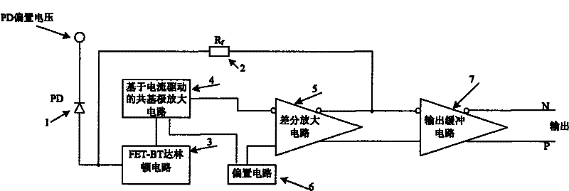
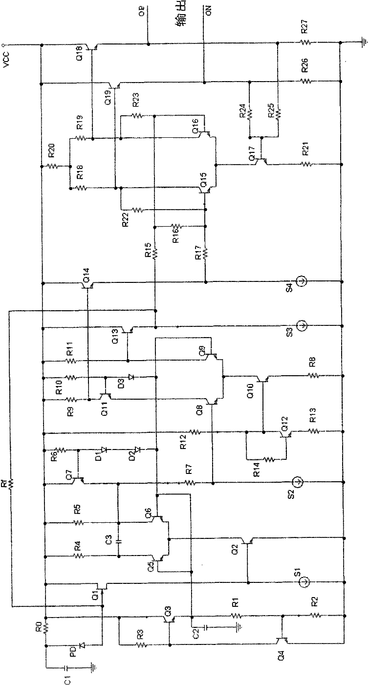
[0034] Please refer to figure 1 , the optical input preamplifier for optical communication receiver provided by the present invention comprises a photodiode 1, a feedback resistor (Rf) 2, a reach by field effect transistor (FET) and bipolar transistor (BT) Linton circuit 3, a current-driven common base amplifier circuit 4, a differential amplifier circuit 5, a bias circuit 6 providing bias voltage, and a differential amplifier circuit 7 with voltage negative feedback.
[0035] The photodiode 1 converts the received light signal into a current signal, and the current signal is converted into a voltage signal through the feedback resistor 2 . The FET-BT Darlington circuit 3 converts the above-mentioned voltage signal into a current signal with a very high transconductance, and injects the current signal into the current-driven common base ampl...
PUM
 Abstract
Description
Claims
Application Information