Method for manufacturing printed circuit board with half-edge hole

A technology of printed circuit boards and half-side holes, which is applied in the fields of printed circuit, printed circuit manufacturing, and multilayer circuit manufacturing. drop effect

Active Publication Date: 2010-04-14
SHENZHEN KING BROTHER ELECTRONICS TECH
View PDF3 Cites 28 Cited by
  • Summary
  • Abstract
  • Description
  • Claims
  • Application Information

AI Technical Summary

Problems solved by technology

[0004] However, the existing method of manufacturing printed circuit boards with half-side holes is

Method used


Image

  • Method for manufacturing printed circuit board with half-edge hole
  • Method for manufacturing printed circuit board with half-edge hole
  • Method for manufacturing printed circuit board with half-edge hole

Examples


Embodiment Construction

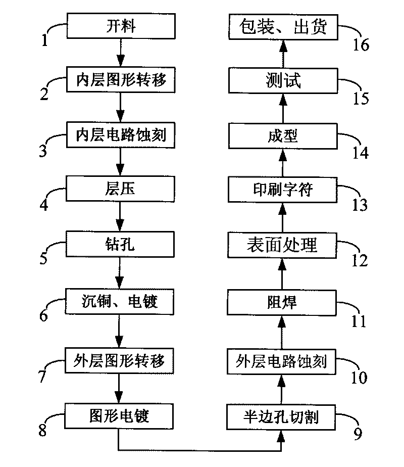
[0024] Embodiments of the present invention will now be described with reference to the drawings, first referring to figure 1 , a method for making a printed circuit board with a half hole in the present embodiment, comprising the steps of:

[0025] (1) The circuit board raw materials of each layer of circuit are cut to form a raw material substrate.

[0026] (2) Transfer the inner layer pattern to each inner layer circuit board to form the inner layer circuit pattern. Since printed circuit boards are usually multi-layer circuit technology, the circuit lines on different layers are different. Therefore, it is necessary to control its circuit lines through the production equipment on each layer, and transfer the inner layer graphics, that is, to make the inner layer circuit graphics.

[0027] (3) Etching the circuit pattern of the inner layer.

[0028] (4) Each layer of the circuit board is then laminated to form a multilayer circuit board.

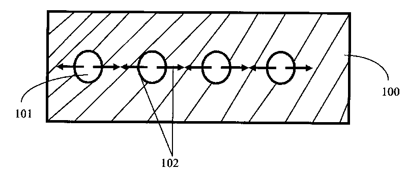
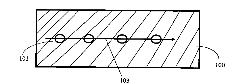
[0029] (5) Drill holes on the c...


PUM


Abstract

The invention provides a method for manufacturing a printed circuit board with a half-edge hole, comprising the following steps: A. implementing inner-layer pattern transfer to a raw material board so as to form each inner-layer circuit and forming a multi-layer circuit board through laminating; B. drilling the circuit board; C. implementing outer-layer pattern transfer to the circuit board and pattern plating; D. forming the half-edge hole by implementing cutting towards the positive and negative directions from the center of a hole when the hole diameter is larger than 1.8mm, while forming the half-edge hole by implementing cutting towards one direction along the center line of the hole when the hole diameter is less than 1.8mm; E. forming an outer-layer circuit by implementing etching; and F. and forming a resistance welding layer on the circuit board by implementing resistance welding printing. The method forms the half-edge hole by implementing cutting towards the positive and negative directions from the center of the hole, thus preventing copper on the wall of the half-edge hole from being pulled off and reducing the generation of burrs/flashes.

Description

technical field [0001] The invention relates to a printed circuit technology, in particular to a method for manufacturing a printed circuit board with a half hole. Background technique [0002] The existing printed circuit boards generally have half-side holes, and the functions of the half-side holes on the printed circuit mainly include: [0003] 1. It is convenient for welding; 2. It can be used to inlay nuts during assembly. [0004] However, the existing methods of manufacturing printed circuit boards with half-side holes tend to cause the copper on the half-side hole walls to be pulled off and produce more burrs / peaks. [0005] In view of the above problems, there is a need for a method of making a printed circuit board with a half hole. Contents of the invention [0006] Based on the deficiencies of the prior art, the purpose of the present invention is to provide a method for manufacturing a printed circuit board with a half hole, which can effectively prevent th...

Claims


Application Information

Patent Timeline
IPC IPC(8): H05K3/00H05K3/46
Inventor 陈裕韬陈东朱占植刘敏唐宏华
Owner SHENZHEN KING BROTHER ELECTRONICS TECH
Why Eureka
Try Eureka