Touch panel, touch electronic device and assembly method thereof

An electronic device and assembly method technology, applied in the direction of electrical digital data processing, instrumentation, data processing input/output process, etc., can solve the problem that the thickness cannot be thinned, the production process yield rate of touch-sensitive electronic devices is not high, touch control In order to reduce the weight of conventional electronic devices, etc.

Inactive Publication Date: 2010-06-09
E-TEN
View PDF0 Cites 3 Cited by
  • Summary
  • Abstract
  • Description
  • Claims
  • Application Information

AI Technical Summary

Problems solved by technology

[0006] The purpose of the present invention is to provide a touch-sensitive electronic device to solve the problem that the touch-sensitive electronic device cannot be thinned
[0007] Another object of the present invention is to provide a method for assembling a touch-sensitive electronic device, so as to solve the problem of low yield of the manufacturing process of the touch-sensitive electronic device
[0008] Another object of the present invention is to provide a touch panel to solve the problem that the thickness of the existing touch panel cannot be thinned

Method used


Image

  • Touch panel, touch electronic device and assembly method thereof
  • Touch panel, touch electronic device and assembly method thereof
  • Touch panel, touch electronic device and assembly method thereof

Examples


Embodiment Construction

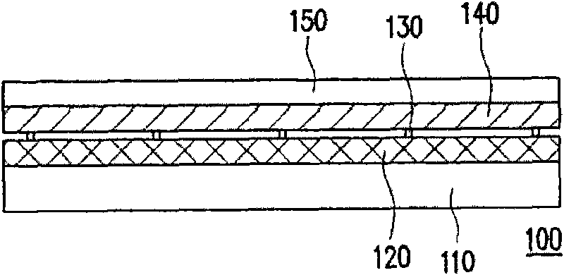
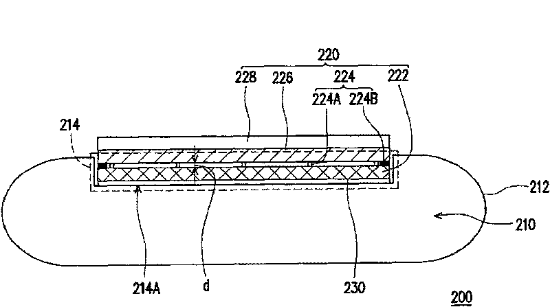
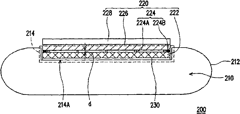
[0042] figure 2 Shown is a touch-sensitive electronic device according to an embodiment of the present invention. Please refer to figure 2 , the touch electronic device 200 includes an electronic device body 210 and a touch element 220 . The electronic device body 210 has an outer casing 212 , and the outer casing 212 has an accommodating portion 214 . In practice, the bottom surface of the accommodating part 214 is a transparent accommodating surface 214A, wherein the accommodating surface 214A can directly constitute a part of the outer shell 212 when the outer shell 212 is formed, or can be pre-formed when the outer shell 212 is formed. After forming an opening at the bottom of the accommodating portion 214 , another transparent material plate is used to cover the opening in a secondary process to form the accommodating surface 214A. The touch element 220 is embedded in the accommodating portion 214 and includes a first conductive film layer 222 , an isolation componen...


PUM


Abstract

The invention discloses a touch panel, a touch electronic device and an assembly method thereof. The touch electronic device comprises an electronic device body and a touch element. The electronic device body is provided with an outer shell which is provided with an accommodating part. In practice, the accommodating part comprises an accommodating face. The touch element is embedded in the accommodating part and comprises a first conducting film layer, an isolating assembly, a second conducting film layer and a protecting film layer. The first conducting film layer, the second conducting film layer and the protecting film layer are sequentially overlapped, and the isolating assembly is positioned between the first conducting film layer and the second conducting film layer for keeping an interval, wherein the first conducting film layer is directly attached on the accommodating face.

Description

technical field [0001] The present invention relates to a touch panel, a touch electronic device and an assembly method thereof, and in particular to a thinned touch panel, a touch electronic device and an assembly method thereof. Background technique [0002] In response to the requirements of modern electronic products to be light, thin and short, all electronic components are actively developing towards miniaturization. Various portable electronic devices have gradually become mainstream, such as personal digital assistants (Personal Digital Assistant, PDA), mobile phones (Cell Phone), and electronic dictionaries. In order to meet the miniaturization requirements of the portable electronic device, each part installed in it must meet the conditions of small size (not occupying space) and light weight, so as to achieve the above-mentioned purpose. [0003] In general portable electronic devices, a touch display panel is usually used as an input medium to achieve the purpos...

Claims


Application Information

Patent Timeline
IPC IPC(8): G06F3/045
Inventor 吕子豪
Owner E-TEN
Why Eureka
Try Eureka