Sensor unit and manufacture method thereof

A manufacturing method and sensor technology, applied to instruments, electrical digital data processing, input/output process of data processing, etc., can solve problems such as increased difficulty of process, complexity of process and structure, overflow of glue, etc., and achieve cost saving , the effect of optimizing reliability

Active Publication Date: 2013-07-03
LITE ON SINGAPORE PTE LTD
View PDF2 Cites 0 Cited by
  • Summary
  • Abstract
  • Description
  • Claims
  • Application Information

AI Technical Summary

Problems solved by technology

However, the above-mentioned structure has the following disadvantages: the packaging structure must be formed with a snap-fit ​​structure to facilitate the assembly of the metal frame, thus increasing the complexity of the process and structure; or glue is applied to the packaging structure to fix the above-mentioned Metal frame, however, the application of glue is not easy to control, too much glue will cause the problem of glue overflow; too little glue, the fixing degree of the metal frame is not good, it is easy to fall off or shift, which will lead to poor signal isolation
[0005] Furthermore, under the trend of reducing the size of components, the metal frame and packaging structure must have a very high precision, so that they can be assembled with each other to form a sensor unit with high isolation effect, so the difficulty of the process is greatly increased, and the product yield rate Can't effectively improve

Method used


Image

  • Sensor unit and manufacture method thereof
  • Sensor unit and manufacture method thereof
  • Sensor unit and manufacture method thereof

Examples


Embodiment Construction

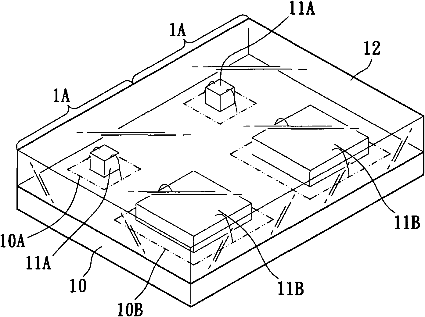
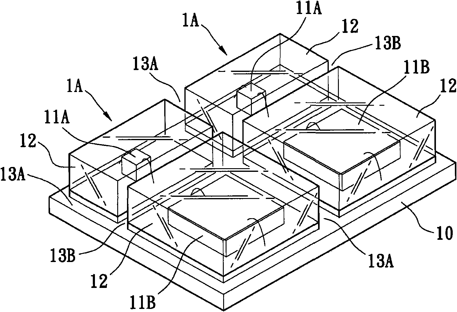
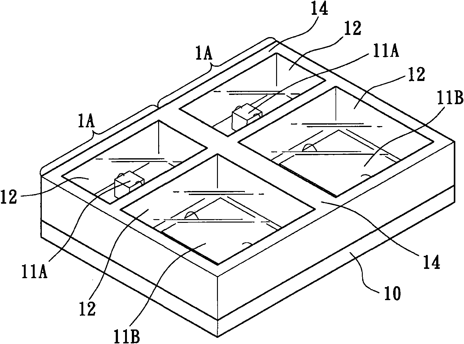
[0022] see Figure 1 to Figure 4 , the present invention provides a manufacturing method of the sensor unit 1, the manufacturing method is to use two molding methods to package and isolate the components of the sensor unit 1, which has the effect of reducing the process cost and can also solve the problem of traditional assembly The absence of the mode, its manufacturing method comprises the following steps:

[0023] The step (1) of the present invention is to provide a substrate 10 including a plurality of sensor regions 1A on the substrate 10 . Such as figure 1 As shown, in this specific embodiment, the substrate 10 includes two sensor regions 1A, and each sensor region 1A will form a sensor unit 1 (such as Figure 4 shown). Each sensor area 1A is provided with two independent circuit areas 10A, 10B on the surface and inside of the substrate 10 (but the number of the circuit areas can be more than two), and in this embodiment, the sensor unit 1 The signal transmitter 11A...


PUM


Abstract

The invention discloses a sensor unit and a manufacture method thereof. The manufacture method of the sensor unit comprises the following steps of: providing a substrate, wherein each sensor region on the substrate is provided with two independent circuit regions on the substrate, and the two circuit regions are respectively provided with a signal emitter and a signal sensor; forming a first package structure on the substrate by using a die to cover the signal emitter and the signal sensor; carrying out first cutting to form a first cutting channel around the two circuit regions and a second cutting channel positioned between the two circuit regions; forming a second package structure in the first and the second cutting channels by using the die; and carrying out second cutting to form a plurality of single sensor units, wherein the second package structure is used for isolating the signal emitter from the signal sensor.

Description

technical field [0001] The invention relates to an inductor unit and its manufacturing method, especially to an inductor manufacturing method using the same mold for two-pass molding steps, and an inductor unit with a high-precision structure. Background technique [0002] With the development of electronic products, many types of input devices are currently available for performing operations in electronic systems, such as buttons or keys, mice, trackballs, touch screens, and so on. Recently, the application of touch screen is more and more common. The touch screen may include a touch panel, which may be a transparent panel with a touch-sensitive surface, so that the working surface covers the viewable area of ​​the display screen. The touch screen allows the user to make a selection and move a cursor by touching the display screen with a finger or a stylus, and perform operations according to touch events. Infrared proximity sensors (IR proximity sensors) are widely used ...

Claims


Application Information

Patent Timeline
Patent Type & Authority Patents(China)
IPC IPC(8): G06F3/041
Inventor 林生兴葛明
Owner LITE ON SINGAPORE PTE LTD
Why Eureka
Try Eureka