Method for producing sensor unit

A manufacturing method and sensor technology, which are used in semiconductor/solid-state device manufacturing, electrical components, electrical solid-state devices, etc., can solve the problems of increased process difficulty, easy falling off or displacement, and overflow of glue, and achieve cost savings and excellent reliability. The effect of high degree and simple process

Inactive Publication Date: 2012-10-17
LITE ON SINGAPORE PTE LTD
View PDF2 Cites 6 Cited by
  • Summary
  • Abstract
  • Description
  • Claims
  • Application Information

AI Technical Summary

Problems solved by technology

However, the above-mentioned structure has the following defects: the manufacture and structure of the metal frame are complex; and the packaging structure needs to be glued, and the above-mentioned metal frame is fixed by glue, but the glue coating is not easy to control, too much glue will Causes the problem of overflowing glue; too little glue, the metal frame is not well fixed, easy to fall off or shift, which will lead to poor signal isolation
[0005] Furthermore, under the trend of reducing the size of components, the metal frame and packaging structure must have a very high precision, so that they can be assembled with each other to form a sensor unit with high isolation effect, so the difficulty of the process is greatly increased, and the product’s The yield rate cannot be effectively improved

Method used


Image

  • Method for producing sensor unit
  • Method for producing sensor unit
  • Method for producing sensor unit

Examples


Embodiment Construction

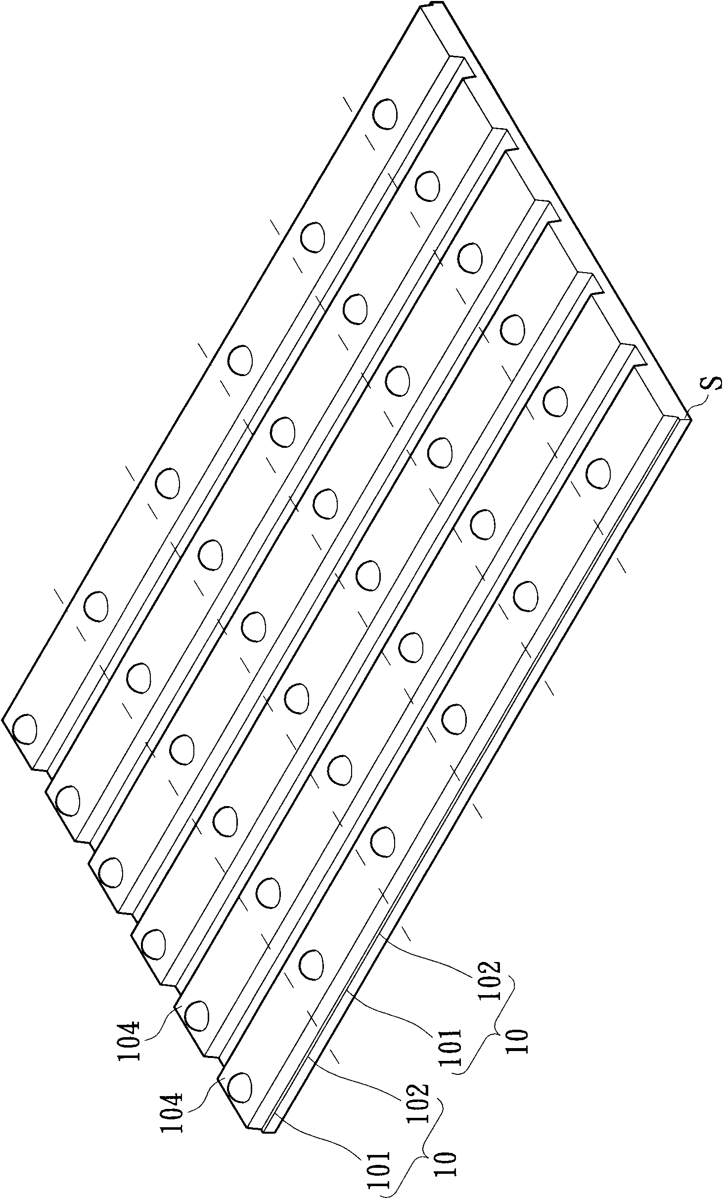
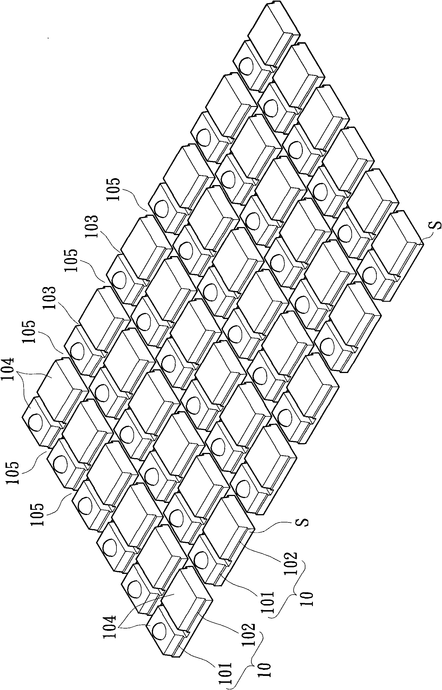
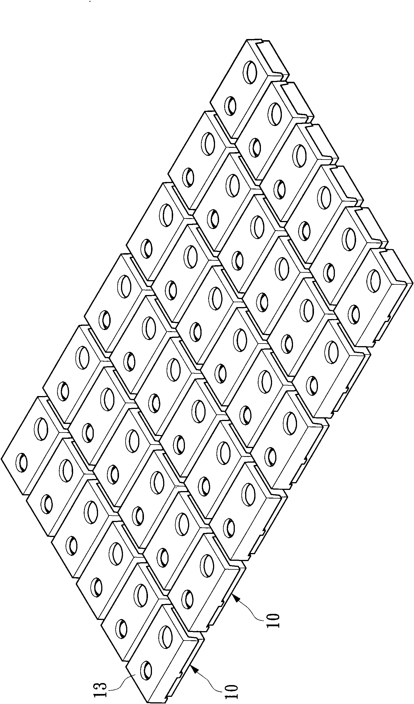
[0035] see Figure 1 to Figure 3 , and with Figure 4 The present invention provides a method for manufacturing the sensor unit 1. The manufacturing method utilizes a one-time modeling method and an assembly spacer 13 to package and isolate the sensor unit 1, which has the effect of reducing the process cost, and more The defect of the traditional assembly method can be solved, and its manufacturing method includes the following steps:

[0036] Step (1): A substrate S is provided, and the substrate S includes a plurality of sensor regions 10 . Such as figure 1 As shown, in this specific embodiment, the substrate S includes an array of 6 by 6 sensor regions 10, and each sensor region 10 will form a sensor unit 1 ( Such as Figure 4 , Figure 5 shown). Each sensor area 10 is provided with two independent circuit areas 101, 102 on the surface and inside of the substrate S (but the number of the circuit areas 101, 102 can be more than two), and in this embodiment, the sensor...


PUM


Abstract

The invention discloses a method for producing a sensor unit. The method comprises the following steps: providing a substrate, each sensor area on the substrate comprising at least two independent circuit areas, and a signal emitter and a signal detector being respectively arranged on the at least two circuit areas of each sensor area; forming a packaging structure on the substrate by utilizing a mould, the packaging structure covering the signal emitter, the signal detector and a cutting area defined between each circuit area; performing a cutting step along the cutting area defined between each circuit area to form separating cut channels between the at least two circuit areas until the substrate is exposed; and assembling a separator on each sensor area, and disposing the separator on the separating cut channel with the substrate exposed to separate the signal emitter and the signal detector in each sensor area. The method is simple in process, and saves costs.

Description

technical field [0001] The invention relates to a method for manufacturing a sensor unit, in particular to a method for manufacturing a distance sensor unit. Background technique [0002] With the development of electronic products, many types of input devices are currently available for performing operations in electronic systems, such as buttons or keys, mice, trackballs, touch screens, and so on. Recently, the application of touch screen is more and more common. The touch screen may include a touch panel, which may be a transparent panel with a touch-sensitive surface, so that the working surface covers the viewable area of ​​the display screen. The touch screen allows the user to make a selection and move a cursor by touching the display screen with a finger or a stylus, and to realize calculation actions according to touch events. Infrared proximity sensors (IR proximity sensors) are widely used in handheld communication devices to detect the distance between the user'...

Claims


Application Information

Patent Timeline
Patent Type & Authority Applications(China)
IPC IPC(8): H01L21/56H01L25/16H01L23/31
CPCH01L2224/48227H01L2224/97
Inventor 林生兴吴德财
Owner LITE ON SINGAPORE PTE LTD
Why Eureka
Try Eureka