Composite thin film solar cell taking microcrystalline silicon layer as incident layer and preparation method thereof

A technology of composite thin film and microcrystalline silicon layer, applied in circuits, capacitors, photovoltaic power generation, etc., can solve the problems of poor liquid stability, high preparation cost, low preparation rate, etc.

Inactive Publication Date: 2011-06-22
HEBEI UNIV OF TECH
View PDF8 Cites 8 Cited by
  • Summary
  • Abstract
  • Description
  • Claims
  • Application Information

AI Technical Summary

Problems solved by technology

[0006] The technical problem to be solved by the present invention is to provide a composite thin-film solar cell and a preparation method thereof, wherein the dye-sensitized nanocrystalline material and the microcrystalline silicon composite thin-film material are directly prepared on a conductive substrate to...

Method used


Image

  • Composite thin film solar cell taking microcrystalline silicon layer as incident layer and preparation method thereof
  • Composite thin film solar cell taking microcrystalline silicon layer as incident layer and preparation method thereof

Examples


Embodiment 1

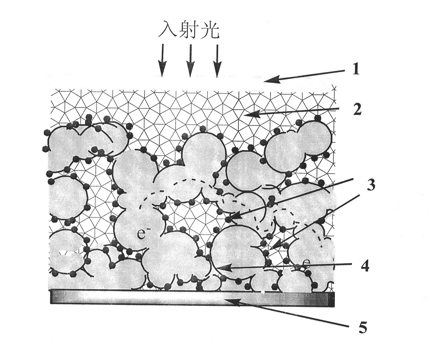
[0067] Solid blackdye dye-sensitized TiO 2 Nanocrystalline composite thin-film solar cells with a microcrystalline silicon layer as the incident layer, and SnO doped with fluorine 2 Conductive layer, microcrystalline silicon hole transport layer, blackdye dye-sensitized TiO 2 nanocrystalline porous membrane and a steel sheet substrate coated with a titanium metal layer, the blackdye dye-sensitized TiO 2 The nanocrystalline porous membrane was coated on a steel sheet substrate coated with a titanium metal layer, and the microcrystalline silicon hole transport layer was deposited on blackdye dye-sensitized TiO 2 Formation of solid-state blackdye dye-sensitized TiO on nanocrystalline porous membranes 2 Composite thin films of nanocrystalline microcrystalline silicon made of SnO doped with fluorine 2 The conductive layer is plated on solid blackdye dye-sensitized TiO 2 Formation of Fluorine-doped SnO on Nanocrystalline Microcrystalline Silicon Composite Films 2 Conductive lay...

Embodiment 2

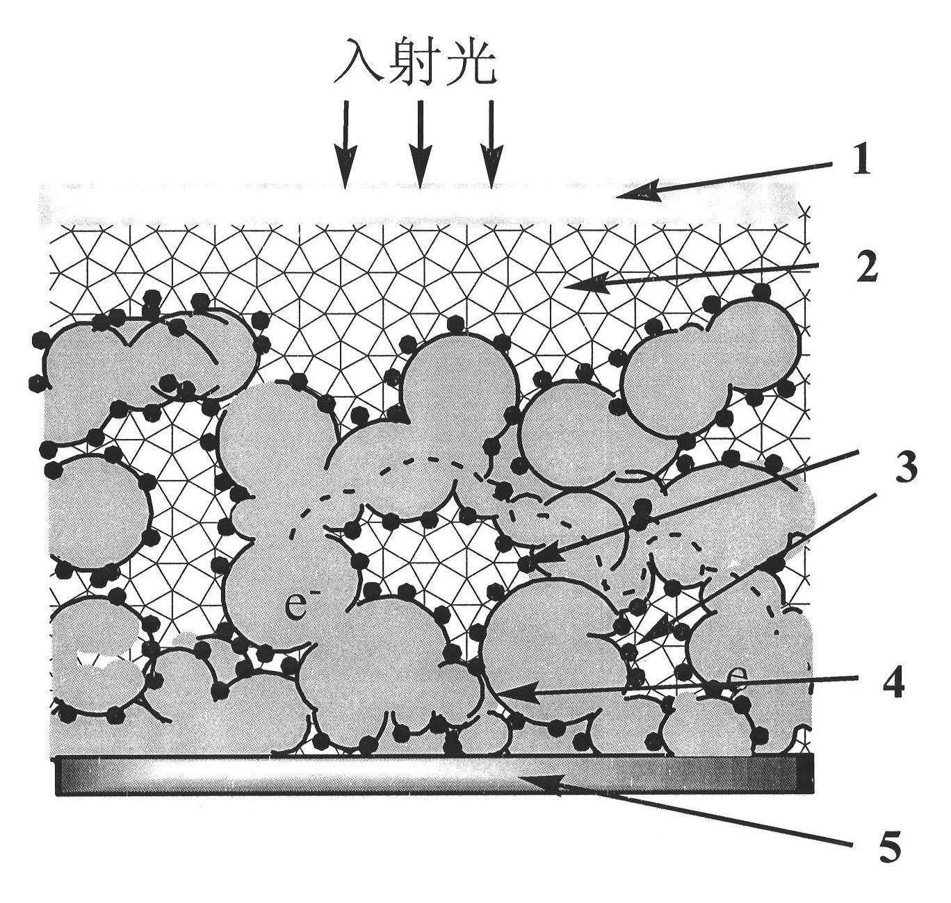
[0086] Solid blackdye dye-sensitized TiO 2 Nanocrystalline composite thin-film solar cells with a microcrystalline silicon layer as the incident layer, and SnO doped with fluorine 2 Conductive layer, microcrystalline silicon hole transport layer, blackdye dye-sensitized TiO 2 nanocrystalline porous membrane and a steel sheet substrate coated with an aluminum metal layer, the blackdye dye-sensitized TiO 2 The nanocrystalline porous membrane was coated on a steel sheet substrate coated with an aluminum metal layer, and the microcrystalline silicon hole transport layer was deposited on blackdye dye-sensitized TiO 2 Formation of solid-state blackdye dye-sensitized TiO on nanocrystalline porous membranes 2 Composite thin films of nanocrystalline microcrystalline silicon made of SnO doped with fluorine 2 The conductive layer is plated on solid blackdye dye-sensitized TiO 2 Formation of Fluorine-doped SnO on Nanocrystalline Microcrystalline Silicon Composite Films 2 Conductive l...

Embodiment 3

[0090] Solid blackdye dye-sensitized TiO 2 Nanocrystalline composite thin-film solar cells with a microcrystalline silicon layer as the incident layer, and SnO doped with fluorine 2 Conductive layer, microcrystalline silicon hole transport layer, blackdye dye-sensitized TiO 2 nanocrystalline porous membrane and a steel sheet substrate coated with a copper metal layer, the blackdye dye-sensitized TiO 2 The nanocrystalline porous membrane was coated on a steel sheet substrate coated with a copper metal layer, and the microcrystalline silicon hole transport layer was deposited on blackdye dye-sensitized TiO 2 Formation of solid-state blackdye dye-sensitized TiO on nanocrystalline porous membranes 2 Nanocrystalline microcrystalline silicon composite thin films, consisting of a fluorine-doped SnO2 conductive layer were plated on solid blackdye dye-sensitized TiO 2 A fluorine-doped SnO2 conductive layer surface electrode is formed on the nanocrystalline microcrystalline silicon c...


PUM

PropertyMeasurementUnit
Thicknessaaaaaaaaaa
Diameteraaaaaaaaaa
Thicknessaaaaaaaaaa

Abstract

The invention discloses a composite thin film solar cell taking a microcrystalline silicon layer as an incident layer and a preparation method thereof, which relate to a special semiconductor device applied to the conversion of luminous energy into electric energy. The composite thin film solar cell consists of a transparent conductive layer, a microcrystalline silicon hole transmission layer, a dye-sensitized nanocrystalline porous film and a conductive substrate, wherein the dye-sensitized nanocrystalline porous film is coated on the conductive substrate, the microcrystalline silicon hole transmission layer is deposited on the dye-sensitized nanocrystalline porous film to form a solid-state dye-sensitized nanocrystalline microcrystalline silicon composite thin film, and the transparent conductive layer is deposited on the microcrystalline silicon hole transmission layer so as to form the composite thin film solar cell taking the microcrystalline silicon layer as the incident layer. A dye-sensitized nanocrystalline material and the microcrystalline silicon composite thin film material are directly prepared on the conductive substrate, so the composite thin film solar cell and the preparation method thereof overcome the shortcomings of dependence of a dye-sensitized solar cell on transparent conductive glass, low preparation rate and high preparation cost of the microcrystalline silicon thin film solar cell, and the low liquid stability of the conventional dye-sensitized solar cell in the prior art.

Description

technical field [0001] The technical solution of the invention relates to a semiconductor device specially suitable for converting light energy into electric energy, specifically a composite thin-film solar cell with a microcrystalline silicon layer as an incident layer and a preparation method thereof. Background technique [0002] The current dye-sensitized solar cell (Dye-sensitized Solar Cell, referred to as DSSC) has achieved a photoelectric conversion efficiency close to that of silicon cells at one-tenth of the cost of silicon cells, and has great application prospects. Traditional DSSCs are mainly composed of transparent conductive glass, porous titanium dioxide film, dye sensitizer, solution or solid electrolyte, and counter electrode. For example, CN201478130U discloses a new structure of a solid titanium dioxide dye-sensitized thin-film solar cell, CN201302932 an electrode structure of a dye-sensitized solar cell, and CN101740238A a dye-sensitized solar cell and i...

Claims


Application Information

Patent Timeline
IPC IPC(8): H01G9/042H01G9/20H01M14/00H01L51/42H01L51/44H01L51/48
CPCY02E10/542Y02E10/50Y02E10/549
Inventor 刘守彬田汉民杨瑞霞田学民王伟杨帆赵红东吕俊李毅杰
Owner HEBEI UNIV OF TECH
Why Eureka
Try Eureka