
Method for manufacturing resistor end effect curves of thick-film integrated circuit

An effect curve, integrated circuit technology, applied in circuits, electrical components, electrical digital data processing, etc., can solve problems such as design errors of thick film resistors, and achieve the effect of improving the level of design technology and ensuring the consistency of resistance values.

Active Publication Date: 2013-04-24
EAST CHINA INST OF OPTOELECTRONICS INTEGRATEDDEVICE
View PDF6 Cites 0 Cited by
  • Summary
  • Abstract
  • Description
  • Claims
  • Application Information

AI Technical Summary

Problems solved by technology

[0005] The present invention is to provide a thick film integrated circuit resistance terminal effect curve production method to solve the problem of thick film resistor design errors caused by layout designers based on the single resistance design curve provided by thick film resistor paste manufacturers

Method used


Image

  • Method for manufacturing resistor end effect curves of thick-film integrated circuit
  • Method for manufacturing resistor end effect curves of thick-film integrated circuit
  • Method for manufacturing resistor end effect curves of thick-film integrated circuit

Examples


Embodiment Construction

[0027] 1. Layout design

[0028] To draw the design curve of the thick film resistor is to make the change curve of the length of the thick film resistor and the resistance value of the thick film resistor. In order to explore the relationship between the length of the thick film resistor and the resistance value of the thick film resistor, the actual product must be prepared. By measuring the resistance value of the thick film resistor of the actual product, the length of the thick film resistor and the resistance value of the thick film resistor can be obtained. change curve. Therefore, in order to prepare an actual product, it is necessary to design a thick film resistor terminal effect curve to make a layout. The specific layout design method is as follows:

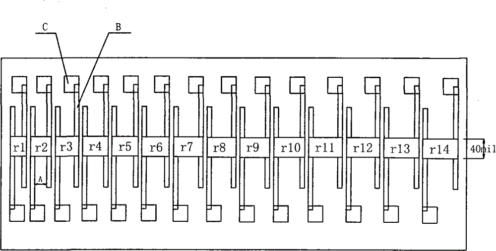
[0029] (1) The layout of the thick film resistor terminal effect curve (resistor width 40mil) is attached. image 3 :

[0030] a. Design conductor layer: used for lap connection of thick film resistor terminals. ...


PUM


Abstract

The invention relates to a method for manufacturing resistor end effect curves of a thick-film integrated circuit, and the method comprises the following steps: a) printing 28 conduction bands B on a film-forming baseplate respectively, wherein spacing intervals A between every two adjacent conduction bands are 15mil, 20mil, 25 mil,..., 70mil, 75mil and 80mil, 14 kinds in total, respectively; b) printing a thick-film resistor r1-r14 with the resistor width of 40mil on the film-forming baseplate respectively; c) using a multimeter to measure the resistance of the thick-film resistor in the film-forming baseplate, recording the measured resistance in an Excel sheet, and getting N which is equal to R / Ri*(W / L) according to the formula that R=Ri*N*(L / W); and d) utilizing the drawing function of Excel to draw a resistor end effect curve map against the different resistor widths respectively. The invention has the following advantages: solving the resistor design error problem caused by the situation that a thick-film slurry manufacturer only provides a single conductor end resistor design curve, improving the design technical level of a thick-film circuit layout, ensuring the resistanceconsistency of the thick-film resistor during the practical processing and enabling the deviation among the resistances of the resistors with the same resistance to be less than 5% when lapping different conductor ends.

Description

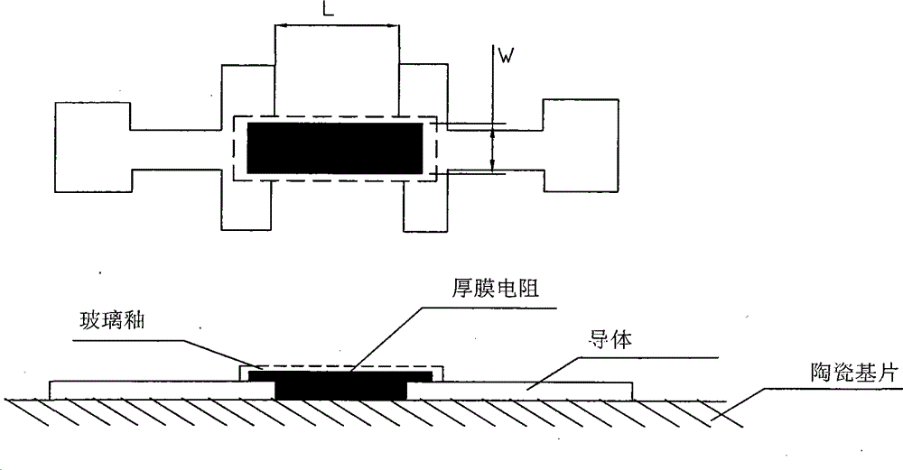
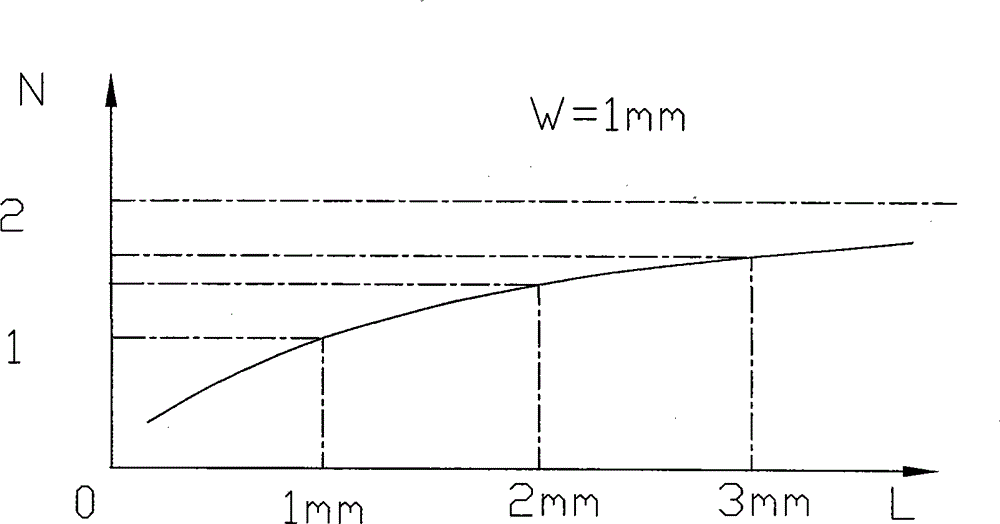
Technical field: [0001] The invention relates to the technical field of thick-film integrated circuit layout design, in particular to a method for preparing a terminal effect curve for thick-film integrated circuit layout resistors. Background technique: [0002] The substrate of the thick film resistor is a ceramic substrate, the electrodes at both ends of the resistor set on the ceramic substrate are conductors, and the surface of the resistor is covered with a layer of glass glaze. See attached for details figure 1 . Design according to the thick film resistor design curve provided by the thick film resistor paste manufacturer. The thick film resistor design curve is obtained when the thick film resistor width is 1mm, where the X-axis is the length of the thick film resistor, and the Y-axis is the variation coefficient N. For details, see the attached figure 2 . [0003] Thick film resistor design calculation formula: resistance value R=R □ · N · (L / W). Square resi...

Claims


Application Information

Patent Timeline
Patent Type & Authority Patents(China)
IPC IPC(8): H01L21/02G06F17/50
Inventor 尤广为王守政鲍秀峰钱嵘卫
Owner EAST CHINA INST OF OPTOELECTRONICS INTEGRATEDDEVICE
Learn More