Thick-film resistor layout design device

A thick film resistor, layout design technology, applied in the direction of calculation, electrical digital data processing, special data processing applications, etc., can solve the problem of lack of design specifications, to eliminate the influence of resistance end effect, solve design deviation, design technology level improved effect

Active Publication Date: 2014-01-08
EAST CHINA INST OF OPTOELECTRONICS INTEGRATEDDEVICE
View PDF1 Cites 0 Cited by
  • Summary
  • Abstract
  • Description
  • Claims
  • Application Information

AI Technical Summary

Problems solved by technology

[0004] The purpose of the present invention is to provide a thick-film resistor layout design device to standardize the thick-film integrated circuit layout design for the shortcomings of existing thick-film integrated circuit layout resistors without design specifications.

Method used


Image

  • Thick-film resistor layout design device
  • Thick-film resistor layout design device
  • Thick-film resistor layout design device

Examples


Embodiment Construction

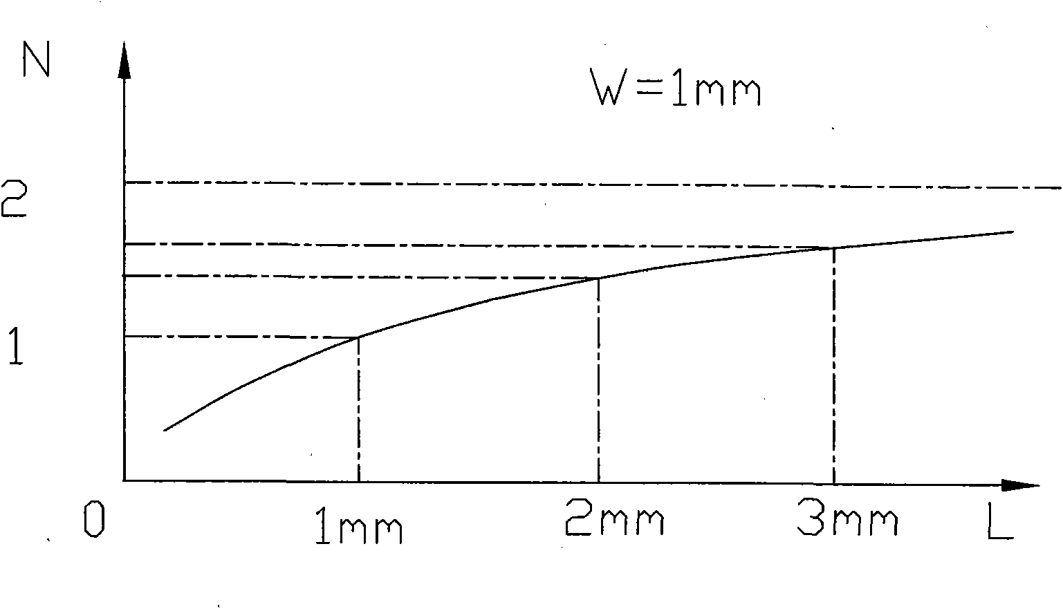
[0029] 1. Determine the end effect curve of thick film resistors

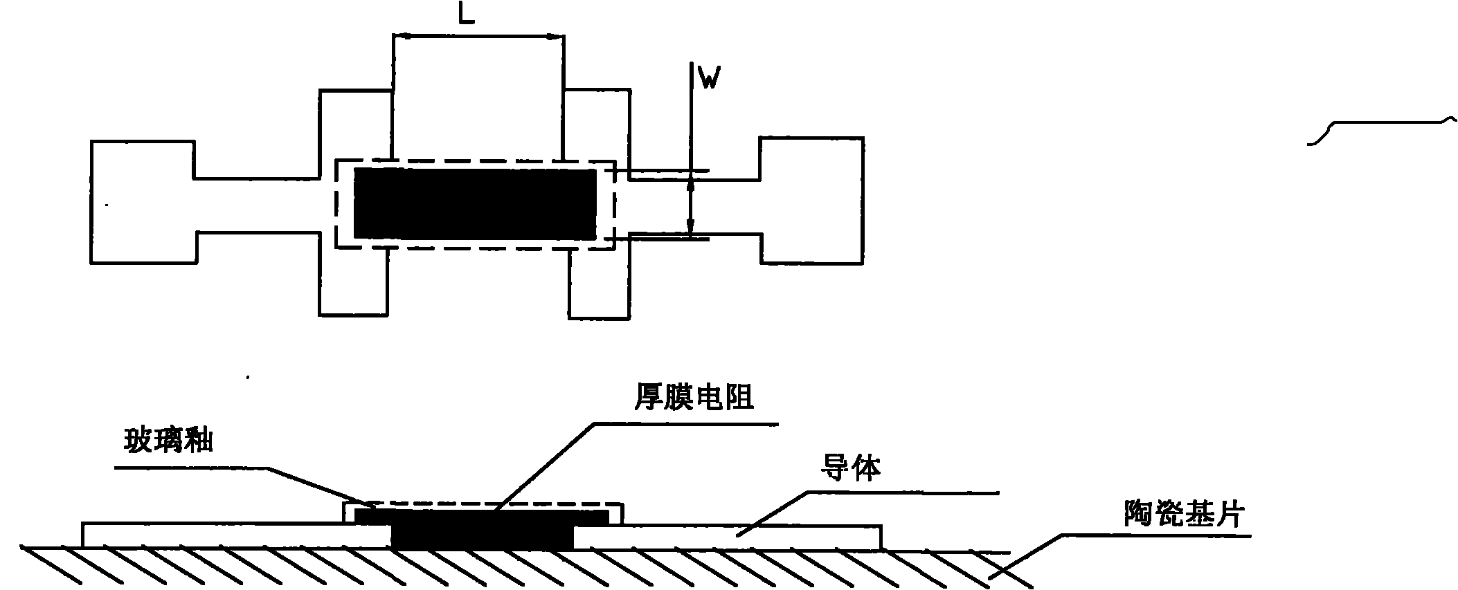
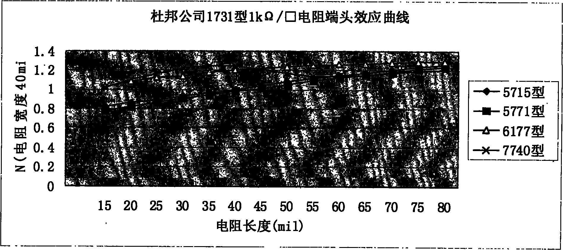
[0030] Necessary conditions for establishing a layout design device for thick-film resistors: According to experiments, the end-effect curves of thick-film resistors (design curves for thick-film resistors at various conductor ends) are obtained. as attached image 3 , Figure 4 It is the tip effect curve of DuPont 1731 type resistor paste.

[0031] 2. Establish a thick film resistor layout design database file

[0032] It is known from the end effect curve of thick film resistors: conductor terminal paste, thick film resistor paste, thick film resistor width, and the one-to-one correspondence between the abscissa L and the ordinate N, we use these information to establish the thick film Resistor layout database files. See the attached block diagram for the specific thick film resistor layout design database structure Figure 5 : Thick Film Resistor Layout Design Database.

[0033] Thick film resistor lay...


PUM


Abstract

The invention relates to a thick-film resistor layout design device which comprises an input device, a CPU, a memory and an output device. The invention is characterized in that the memory is provided with a thick-film resistor layout design database (1), a parameter input module (2) and a function operation module (3), wherein the parameter input module comprises an end conductor material selection module a, a resistor paste sheet resistance selection module b, a thick-film resistor width selection module c and a thick-film resistor target value selection module d; and the function operation module (3) comprises an N.L theoretical value computation module a, an N.L value searching module b, an N.L value comparison module c and a resistor designed length value output module d. The invention can be used for quickly obtaining the design sizes of various thick-film resistors, eliminating the end effect influences on the resistor, and solving the problem of design deviation caused by different N values, thereby enhancing the level of thick-film circuit layout design technique. The invention ensures the resistance consistency of the thick-film resistor during actual machining, so that the resistance deviation among resistors which have the same resistance and are overlapped on different conductor ends is less than 5%.

Description

Technical field: [0001] The invention relates to the technical field of layout design of thick-film integrated circuits, in particular to a device for layout resistance design of thick-film integrated circuits. Background technique: [0002] The substrate of the thick film resistor is a ceramic substrate, the electrodes at both ends of the resistor set on the ceramic substrate are conductors, and the surface of the resistor is covered with a layer of glass glaze. Design according to the thick film resistor design curve provided by the thick film resistor paste manufacturer. The thick film resistor design curve is obtained when the thick film resistor width is 1mm, where the X-axis is the length of the thick film resistor, and the Y-axis is the variation coefficient N. For details, see the attached figure 2 . Thick film resistor design calculation formula: resistance value R=R □ · N · (L / W). Square resistance R □ is the resistivity of the thick film resistor at a dry thi...

Claims


Application Information

Patent Timeline
Patent Type & Authority Patents(China)
IPC IPC(8): G06F17/50
Inventor 尤广为王守政鲍秀峰钱嵘卫
Owner EAST CHINA INST OF OPTOELECTRONICS INTEGRATEDDEVICE
Why Eureka
Try Eureka