Pixel array substrate display panel

A pixel array and substrate technology, which is applied in the field of pixel array substrates and display panels with double-layer wiring, can solve the electrostatic damage of peripheral wirings, the great difference in the spacing of peripheral wirings, and the hardening degree of ultraviolet curing sealant. problems, achieve high process compatibility, avoid different degrees of sealant hardening, and reduce the probability of electrostatic damage

Inactive Publication Date: 2011-09-14
CPT TECH GRP +1
View PDF4 Cites 29 Cited by
  • Summary
  • Abstract
  • Description
  • Claims
  • Application Information

AI Technical Summary

Problems solved by technology

However, in the conventional double-layer routing technology, the problem of electrostatic damage often occurs between two adjacent peripheral traces, and because the distance between the peripheral traces is very different, the substrate is damaged due to the difference in the layout of the peripheral traces. Different light transmittances lead to different degrees of hardening of the UV curing sealant coated on the peripheral wiring during the subsequent sealant manufacturing process, which in turn makes the display panel prone to liquid crystal contamination and unable to pass the pulling force Test (tensile test) and other issues

Method used


Image

  • Pixel array substrate display panel
  • Pixel array substrate display panel
  • Pixel array substrate display panel

Examples


Embodiment Construction

[0060] The present invention will be further elaborated below in conjunction with the accompanying drawings.

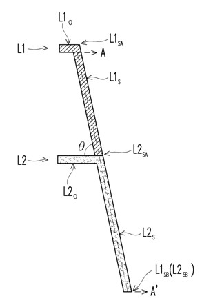
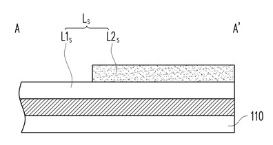
[0061] Figure 1A It is a schematic top view of a pixel array substrate according to an embodiment of the present invention. Please refer to Figure 1A , The pixel array substrate 100 of this embodiment includes a substrate 110, a plurality of pixel structures 120, a plurality of first wires L1 and a plurality of second wires L2.

[0062] The substrate 110 of this embodiment includes a display area R1 and a peripheral circuit area R2, and the peripheral circuit area R2 is located outside the display area R1. In this embodiment, the display region R1 is, for example, a rectangular region, and the peripheral circuit region R2 has adjacent frontal region R2A and terminal region R2B corresponding to the adjacent two sides S1 and S2 of the display region R1, and the frontal region R2A is connected to terminal area R2B. In this embodiment, the substrate 110 is used to car...


PUM


Abstract

The invention relates to a pixel array substrate which comprises a substrate, a plurality of pixel structures, a plurality of first routings and second routings, wherein the substrate comprises a display area and a peripheral circuit area out of the display area, the pixel structure array is arranged in the display area, the plurality of first routings and second routings are located at the peripheral circuit area, and respectively electrically connected with the corresponding pixel structure; the second routing is above the first routing and electrically insulated from the first routing; the first routing and the second routing are respectively extended along a column direction from the display area and alternatively arranged on a line direction; the projections of each first routing and one of the adjacent second routing are crossed and overlapped with each other by means of inclined parts with the same slope so as to form a set of double-layer routing; and furthermore, the invention provides a display panel with the pixel array substrate. The narrow side of the pixel array substrate can be framed so as to improve the problem of static damage of two adjacent peripheral routings in the traditional pixel array substrate.

Description

technical field [0001] The present invention relates to a pixel array substrate and a display panel, and in particular to a pixel array substrate and a display panel with double-layer wiring. Background technique [0002] With the vigorous development of display technology, display panels have been applied to display devices of various sizes, such as televisions, computer screens, notebook computers, mobile phones, and the like. Taking mobile phones as an example, consumers not only have requirements for the display performance of the display panel, such as resolution, contrast, viewing angle, etc., but also have increasingly higher requirements for the aesthetic appearance of the display panel. Therefore, many manufacturers related to display panels have invested in narrow bezel (slim boarder) display panels one after another, so that display panels with the same display quality are thinner, lighter and smaller to meet consumer demand. [0003] In order to realize a displa...

Claims


Application Information

Patent Timeline
Patent Type & Authority Applications(China)
IPC IPC(8): G02F1/1362G02F1/1368H01L27/02
Inventor 林圣佳江佳铭
Owner CPT TECH GRP
Why Eureka
Try Eureka